Researchers at the University of New South Wales (UNSW) in Australia have taken a significant step in the development of so-called ferroelectric domain wall (FEDW) memories. These results could lead to a non-volatile memory with a higher storage density than traditional memory devices and be the realization of the unfulfilled promise presented by magnetic domain wall memory, also known as “racetrack memory”.
Nearly a decade ago, Stuart Parkin and his colleagues at IBM Almaden Research demonstrated a three-bit version of so-called “racetrack memory.” Racetrack memory is a solid-state non-volatile memory that promised much higher storage density than conventional solid-state memory devices.
It was expected to be a truly disruptive alternative memory technology, but it turned out to be about a thousand times slower than anticipated, putting it on par with the performance of traditional hard drives.
While racetrack memories are based on nanowires made from ferromagnetic materials that can have their magnetization switched through an applied magnetic field, FEDW memories are made from ferroelectric materials whose electric field polarization is changed via an electric field.
In research described in the journal Science Advances, the UNSW scientists fabricated a memory device from these ferroelectric materials and have demonstrated that it can operate at relatively low voltages (less than 3 volts). It also has a relatively high OFF-ON ratio, making it easier to assign a “0” and “1” to distinct ferroelectric states.
“The domain walls we investigate and use here are ferroelectric walls, not magnetic walls,” said Jan Seidel, associate professor at UNSW and co-author of the research, in an e-mail interview with IEEE Spectrum. “While you have oriented spins in a magnet, you have oriented electric dipoles in a ferroelectric materials, so this is, in some sense, the electric equivalent of a ferromagnet.”
One of the benefits of ferroelectric domain walls is that their width is anywhere from 10 to 100 times smaller than conventional magnetic walls. That makes them the ultimate nanoscale controllable feature in solid materials, according to Seidel. Because the walls are so thin, you can encounter structural changes and symmetry changes of the material, which can drastically alter the material’s property.
“You can think of the wall potentially being a completely different material,” explained Seidel. “This is the key point we use in our memory cells. The domain walls are electrically conductive, while the wall’s surroundings (the bulk of the material) is insulating.”
Because the electric dipoles (positive and negative charges) in ferroelectrics can be influenced and reoriented by external electric fields (applied voltage), walls can be created, erased or relocated in the material. This method of creating and erasing walls makes it possible to form or take away conductive channels in which data is stored.
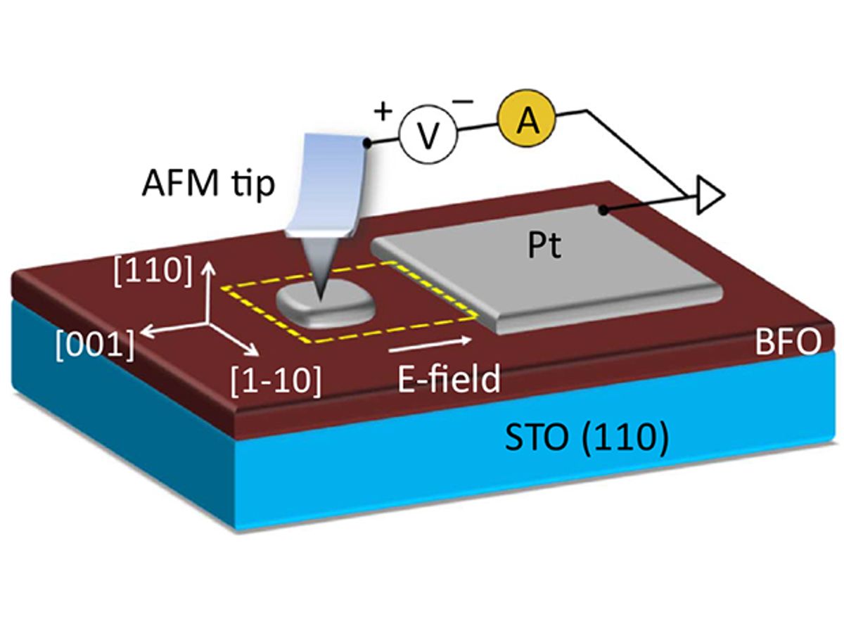
Seidel and his UNSW colleagues fabricated their prototype FEDW device with bismuth ferrite (BFO) thin films that are grown on a strontium titanate (STO) substrate. The BFO thin films—at least the type produced here—possess a near mono-domain state, providing a clean slate for creating and erasing different domain walls.
To ensure that a steady current was applied to the device, the researchers placed nanofabricated platinum/titanium electrodes (a big one and a small one) on the same plane as the BFO thin film. This in-plane geometry of the electrodes makes it possible to encode and retrieve information through moderate electric fields rather than electric currents, leading to low-energy operation.
“A key point in our research is that we have found a way to stabilize the domain walls on the nanoscale by using the right electrode geometry tailored to the specific materials properties at hand,” explained Seidel.
In this configuration, the large electrode is grounded, while the small electrode serves as the target for the tip of a conductive atomic force microscope. This provides the steady current that triggers a specific FEDW configuration. This design is a major departure from previous FEDW memory designs that exploited in-plane geometry.
While magnetic domain walls have been investigated heavily for memory and logic applications over the past 10 years, work on ferroelectric domain walls is more recent, but is now seeing significant attention, according to Seidel.
Seidel adds: “Much of the work at the moment is fundamental research, but proposals for commercialization have been discussed and are being actively explored. I think we are laying some of the groundwork at the moment for potential industrial uptake of our ideas and concepts.”
Dexter Johnson is a contributing editor at IEEE Spectrum, with a focus on nanotechnology.


