Skip to Main Content

Design Exploration of RF GaN Amplifier, 3D Packaging, and Thermal Analysis

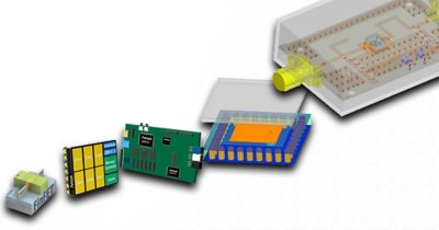
Join us for this webinar on RF GaN amplifier design using electromagnetic/thermal 3D solvers. We will discuss the step-by-step process of building a GaN amplifier, beginning with the transistor model in the circuit simulator. The webinar will outline the steps required to convert this to a physical layout for electromagnetic simulation and verification while integrating packaging and thermal effects co-simulation to analyze a complete packaged system. Discover how this comprehensive approach yields innovative solutions, important design insights, and their potential impact on packaged performance.

Venue:
Digital

Watch Presentation

This site is protected by reCAPTCHA and the Google Privacy Policy and Terms of Service apply.

What You Will Learn

  • Design and layout of a typical GaN amplifier using circuit
    and 3D EM tools
  • Incorporation of 3D component models (connectors, packages etc) for complete system analysis
  • Co-simulation of packaged devices with thermal solvers

Who Should Attend

  • Electromagnetic and circuit design engineers: Delve into the co-
    simulation nuances between circuit models and full 3D designs
  • System engineers: Develop an understanding of the packaged PA design and tradeoffs
  • Professionals in wireless communication: Gain comprehensive
    insights into the modern circuit/package co-simulation
    workflows

Speaker

David Edgar, Senior Manager Applications Engineer

2023-5g-workflow-webpage.jpg