
The last decade saw a surge in the number of small IC design houses that provide systems manufacturers with application-specific ICs (ASICs). These fabless enterprises, so-called because they farm out IC fabrication to commercial silicon chip foundries, cost relatively little to start up yet can be richly rewarded if the market adopts their products. Sustained by a wealth of design tools, they have earned a place alongside long-established, large chip manufacturers like IBM, Intel, Motorola, and Texas Instruments.
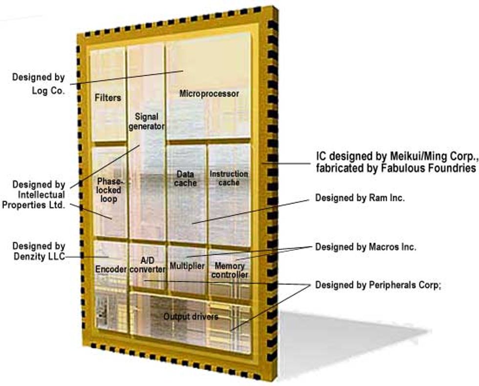
More recently, shrinking circuit features and rising transistor density have spawned the astonishing system on a chip (SoC)[see Fig. 1], in which most or all of the circuitry required for, say, a cellphone fits on a single IC. Today, these SoCs often contain analog, RF, and mixed-signal components to satisfy the growing demands of communication applications.
All the same, the ambitious SoC endeavor risks suffocation by its own success: the number of deployable transistors on a chip far exceeds the design team's power of arranging them to perform meaningful functions. Evidently, SoC designers need input from the intellectual property (IP) providers that design circuit modules for use with other SoC elements. Also, they need design tools that can rapidly integrate IP libraries with the mundane sizing, placing, and routing of circuits.
In short, electronic design automation (EDA) must do more than keep pace with fabrication technology. It must also come to terms with three disruptive changes already molding its prospects and, by extension, those of the larger IC manufacturing sector. First, there is the growing intricacy of SoC and system-in-a-package applications, especially those with large blocks of analog and RF components. Second, there is the need for fabless semiconductor companies to develop business models for sending IP-based designs to foundries or contract manufacturers.v Third, SoC designers require new integrated hierarchical design flows (running from high-level concepts to netlists and wired gates) that allow IP creation and wide reuse. Taken together, the answers to these needs will mold how SoC and ASIC innovations will be captured and exploited by very large-scale circuitry. And EDA tools are essential to the rapid and inexpensive delivery of semiconductor IP to the IC design house, even for low-volume applications.
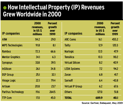
Profits and enormous market growth lie ahead. Commercial IP is one of the most flourishing sectors of the US $800 billion IC market. Consisting of logic, memory, and processor cores developed by third parties for reuse by small design houses and big IC manufacturers, it totaled $690 million in 2000, or 48 percent more than in 1999. The ideal is to enable designers to rapidly plug together an SoC from mix-and-match products made by different IP vendors [see table, below].
The appetite for systems on chips
Heralded by many as the Holy Grail of system design, SoCs unite multiple subsystems, saving circuit board space and power and enhancing performance. In 1995, SoCs had hundreds of thousands of gates, a single programmable microprocessor core, and on-chip memory. Today, the digital, analog, and RF functions found on a single chip are far more diverse. A good instance is the super optical-disk controller for DVD systems developed by Matsushita, of Osaka, Japan. This SoC combines the contents of three chips in one, reducing the power and space requirements while more than doubling playback speed.
An SoC comprises cells and potentially reusable IP blocks that can be recycled from application to application. Examples include digital signal-processor cores like the TMS320C55x family from Texas Instruments and the ADSP-21535 from Analog Devices. Memory subsystems can also be purchased from third-party vendors as blocks for embedding into the SoC.
To facilitate IP portability, the SoC industry founded the Virtual Socket Interface Alliance (VSIA) in 1996. The alliance promotes the mix and match of IP from multiple sources, as well as simplifying the development of stimulus-response checks called test benches. Using the concept of virtual sockets, which define standard interfaces, pre-verified IP can, in principle, be assembled on both a functional and a physical level. In other words, the parts will both play together electronically as a system and fit together on a chip.
To ensure high reliability, VSIA recently formed a study group from representatives of seven organizations (ARM, Fujitsu, IC-Cad Solutions, Intel, the VSIA Japanese Special Interest Group [JSIG], Mentor Graphics, and Synopsys). Their goal is to formulate a comprehensive approach to measuring the factors that determine IP and SoC quality. The factors include design authoring (which defines and documents the arrangement and interaction of functional blocks), design verification, system-level validation, manufacturing, and development of process maturity.
In fact, VSIA's 10th Development Working Group is a quality study group that among other things focuses on how best to implement communications and interfaces, conduct verification, quantify signal integrity, and protect IP developers against unauthorized use of their designs. Consequently, IP providers as well as IP integrators will be able to use common attributes to speedily assess the quality of single IP blocks or entire SoCs.
Key constraints
The shorter a product life cycle, the greater the pressure on the SoC design process to meet time-to-market and time-to-volume goals. Digital IC designs of medium complexity may have found 18-24 months ample for development to market; but now only six months are allowed for multimedia, wireless, and cryptography designs of highly complex SoCs having analog elements.
Consider that a 20-month development phase for a design team of 10 engineers can exceed $225 000 per engineer per year for salaries and overhead alone, translating into development costs of roughly $4.5 million. Clearly, a shorter time to market will cut costs on the front end, as well as generate larger revenues over the longer term. And productivity will be enhanced through improvements to existing EDA tools, new ways of utilizing these tools, and wide deployment of reusable IP into the SoC.
For SoCs of up to medium complexity, computer-aided design tools are widely used to optimize design flow. But it is often difficult, at times impossible, to map complex system requirements comprehensively into a synthesizable high-level architecture. So EDA tools must make doubly sure that the designer's space, power, and timing constraints can be met prior to fabrication.
Another challenge arises from incorporating analog functions into the digital design flow. Conservative predictions indicate that such SoCs will have grown from below 20 percent of the total SoC count in 1997 to more than 60 percent by the end of this year, surpassing $22 billion in total mixed-signal IC revenue. This is obviously a commercial incentive.
The world of analog (low- and, increasingly, high-frequency) circuits is less structured than the digital--hence the paradigm shift presently reshaping the EDA industry. Whereas design flow has centered on the ever-increasing performance of digital components, the revised methodology must systematically embrace both digital and analog components and also take full advantage of reusable IP.
A case in point involves two companies from San Jose, Calif.: inSilicon Corp., a provider of wired and wireless IP communication circuits, and SoC developer Palmchip Corp. The pair has teamed up to provide application-specific SoCs. InSilicon's IP portfolio bulges with more than 700 analog and mixed-signal IP cores. The company's IP will be used in CoreFrame, Palmchip's on-chip interconnect architecture whose synthesis-friendly environment facilitates the plug-and-play of IP from many sources.
Generically speaking, the design flow of the future identifies filters, amplifiers, and phase-locked loops as blocks, each of which is refined into its constituents--so-called standard macro cells like comparators and inverters--eventually arriving at the physical transistors, resistors, capacitors, and inductors. At each level of refinement, a top-down synthesis is executed followed by a bottom-up layout and verification loop. This process establishes specifications for the next lower level of granularity--the partitioning of a macro into smaller entities, called sub-blocks--and constraints on each block to be passed on to the next level [see figure].
Key design flow details must change, too. At present, for instance, synthesis tools incorporate statistical models of wire-loads that assign lumped-circuit parameters such as capacitance and resistance to the interconnects; this accounts for parasitics and load-dependent timing constraints. But the migration to deep-submicron technology and smaller gate widths demands full-wave solutions instead.
Mix-and-match intellectual property
The capital needed to underwrite a complex SoC design and fabrication process is prohibitive, and only the largest IC manufacturers can afford to operate their own foundries. Soon, with new plants approaching $2.5 billion apiece, owning a dedicated facility will become even harder for many chipmakers to justify. These fixed costs have led almost by themselves to the emergence of dedicated foundry services, whose sole business is custom (and high-volume) IC manufacturing. The first commodity foundries like UMC and TSMC appeared in the early and mid-1980s. These pure-play foundries build 12 percent of all ICs today, and are predicted to reach 26 percent by 2004.
Accordingly, small, mid-size, and even large companies like Motorola, LSI Logic, Chip Express, and Samsung are relying less on in-house foundries. Instead, they offer customers their expertise in planning, design, assembling, and testing and leave the burden of IC manufacturing to dedicated, pure-play foundries such as TSMC, Chartered, UMC, and Siterra. In fact, Motorola's Semiconductor Products Sector plans to outsource half its off-the-shelf chip production by the end of 2002. Yet as recently as 1998, less than 6 percent of its chips were manufactured outside.
These fabless businesses have compelling advantages. Without huge fixed foundry costs, even low SoC production volume turns a profit. Design methods can be adopted from those EDA suppliers that offer the best single-purpose, or point, solutions. And as a third party slotted between customer and foundry, the fabless business has no conflict of interest; IP can be procured and fabricated to best solve the technical objectives.
On the downside, fabless SoC design houses could lack for foundry capacity. While not an issue at present, with total foundry utilization at an all-time low of less than 40 percent, it may become one. One remedy is to form strategic alliances with foundries, and even acquire partial ownership of them, so as to ensure a say in capacity allocation. Nonetheless, designing SoCs through third-party EDA tools, purchasing or licensing IP, and outsourcing the IC manufacturing requires a cohesive, highly complex business model.
IP design opportunities
The IP embodied in synthesized circuits may be divided up into functional blocks for use in different designs and for different applications. The first design groups to realize the benefits of reusable IP were the large IC manufacturers. In the mid-1990s, Intel, ARM, and MIPS Technologies began developing embedded processor cores with instruction sets tailored to the application. Worldwide standardization initiatives such as the System Level Design Language (SLDL), which streamlines IP authoring and SoC integration processes, and VSIA's Virtual Component Interface standard, which supplies well-defined and open data communication protocols between blocks of IP, encourage this trend.
Today, a growing number of IP vendors are offering a wide range of mostly embedded components for digital reuse. Bought off the shelf and integrated into an SoC, these components can make designers an order of magnitude more productive. Moreover, once there is general use of embedded reprogrammable logic to customize an IP block, it will be easier to retarget IP blocks for other specific applications, further enhancing productivity.
Mixed-signal properties
Whereas digital IP processes binary signals, analog IP operates on continuous signals whose voltage is precisely specified. This is an even harder problem for the SoC design houses. For one thing, the hardware description languages used for digital designs contain synthesizing options that cannot be used to create analog blocks. With the arrival in the last few years of VHDL and analog and mixed-signal tools like Varias from Avanti, AMSDesigner from Cadence, and Advance-MS from Mentor Graphics, digital and analog signal responses can be simulated. But the simulation is rudimentary, capable only of switching between the HDL digital description and the Spice-based analog circuit model.
Remember, too, that an analog system is specified by such parameters as gain, noise, slew rate, and common-mode rejection. Accordingly, overall IP performance depends much more on the manufacturing process than does a digital design. For that reason, any reusable analog IP is provided in hard form: it is delivered as a physically laid-out and routed circuit, which is added to the rest of the design.
The combination of reusable analog and digital IP will gain ground generally. IP is already found in 25 percent of today's SoCs, and that could triple within five years. The analog portion may already absorb more than half the design effort. Especially for fabless companies, retargeting and reusing analog IP will be a prerequisite for success. Recognizing this trend, TSMC as the world's largest pure-play foundry has already shipped process data of its 0.18-µm CMOS technology to a few providers of analog EDA synthesis tools. Such process information is crucial if analog libraries are to be linkable to the underlying physical deep-submicron technology.
To enhance productivity, third-party vendors of IP will have to offer digital as well as analog and mixed-signal IP as standard libraries, integrated into EDA design flows. As for the tool sets used by design houses, they will have to be flexible enough to manage concurrent hardware-software co-designs. Linear, top-down design flows and the separation of software and hardware design will be things of the past. With the new design flow, designers may use performance as their criterion for partitioning the SoC into hardware and software components and for incorporating digital and analog reusable IP to speed up the design process. The IP will be supplied through standard interfaces, or wrappers, with plug-and-play functionality.
While most engineers view such developments as a distant dream, a small group hails the availability within two or three years of predesigned, preverified, plug-and-play IP cores. They expect the IC design houses could quickly place and route these cores into a standard SoC template for their customers' applications. After all, they can point to the already posted Design and Reuse IP catalog (www.us.design-reuse. com) of Design-Reuse of Newark, Calif., and Grenoble, France, with more than 1700 cores from 190 companies. While the catalog is not as extensive on the analog side and lacks plug-and-play IP capabilities, it indicates how the IP market will evolve.
Next-generation IC technology with 0.1-µm channel size can lead to a lengthy production process: the masks alone take three months to create, and cost over $800 000 each. Costs go even higher when masks require extra features to accommodate the analog portion of a mixed-signal chip. Then, too, the proliferation of 300-mm wafers will raise economy-of-scale issues, as design houses get better at anticipating customers' needs and automate manufacture to effectively populate the wafer. Indeed, larger wafers could become a problem for fabless companies that need only small batches of chips to supply a niche market; they may instead have to turn to more generic, application-specific, reconfigurable, and retargetable systems. And these needs will of course require ever more integration and innovation from the design tool vendors.
--Linda Geppert, Editor
About the Authors
PETER LEVIN (M) & REINHOLD LUDWIG (SM) are both associated with Techno Venture Management (TVM), an international private equity investment firm with offices in Munich, Boston, and San Francisco. Levin is a partner in the firm, and Ludwig serves as a technical advisor to the company. Ludwig is also a professor of electrical engineering at Worcester Polytechnic Institute.
To Probe Further
The International Technology Roadmap for Semiconductors (https://public.itrs.net) provides one of the most comprehensive reviews of future developments in the electronic design space.
For information about analog circuit synthesis tools, check out the Web site of Neolinear Corp. , Pittsburgh (www.neolinear.com), one of the leaders in analog, mixed-signal, and RF designs.
A host of useful white papers on the current state of electronic design can be found on Cadence's Web page (https://www.cadence.com).
For a detailed look at how a complex system on a chip (SoC) is created, refer to "A mixed-signal 0.18-µm CMOS SoC for DVD systems with 432-MSample/s PRML read channel and 16-Mb embedded DRAM," a DVD system on a chip described by T. Yamamoto and his colleagues in the IEEE Journal of Solid State Circuits, Vol. 36, No. 11, pp. 17851793, November 2001.