The Conversation (0)

Illustration: Bryan Christie Design
Remember when combining a camera with a cellphone seemed daring? Or adding a cellphone to a PDA? Such technical tricks relied on Moore’s Law, which holds that the number of transistors on an IC doubles every 18 months. In the computing world, having more transistors on a chip means more speed and possibly more functions.But in many cases, those Moore’s Law ICs deal with only 10 percent of the system. The other 90 percent is still there, showing up as an array of bulky discrete passive components—such as resistors, capacitors, inductors, antennas, filters, and switches—interconnected over a printed-circuit board or two. Real miniaturization requires something more, and we have it in the system-on-package (SOP) approach we’re pursuing at the Microsystems Packaging Research Center at the Georgia Institute of Technology, in Atlanta. SOP leapfrogs well beyond Moore’s Law. It combines ICs with micrometer-scale thin-film versions of discrete components, and it embeds everything in a new type of package so small that eventually handhelds will become anythingfrom multi- to megafunction devices. SOP products will be developed not just for wireless communications, computing, and entertainment. Outfitted with sensors, SOPs could be used to detect all manner of substances, toxic and benign, including chemicals in the environment, in food, and in the human body.
This last application will see the convergence of biology, chemistry, and digital technology to produce capsules small enough to be introduced into the human body to monitor personal health daily. A capsule could be used, for example, to check vital signs and monitor parameters such as glucose levels, blood pressure, and even signs of cancer. The capsule would then wirelessly communicate the person’s health status to a Web terminal outside the body or, via the Internet, to a physician (or to anyone, anywhere). Fitted with a reservoir, the capsule could also deliver drugs at programmed intervals to selected places within the body.
That tiny body capsule is certainly a compelling product, and we can expect many others. Imagine, for example, a home entertainment and control hub—a device that combines voice, video, data, sensing, and control functions. It could include a home computer, a cellphone, environmental and other sensors, a health monitoring device, and a satellite TV receiver, to name just some possibilities. A wireless broadband connection would link the system to the Internet, and the hub would serve as the remote control for all the home’s appliances.
Yet the hub would be as small as a credit card.
We envision a megafunction SOP unit built with microscale components that would be the size of an Intel Pentium processor, which comes in a flat pack 35 centimeters on a side. Or, built with nanoscale technologies, an SOP could be as small as a millimeter on a side. SOP products will attain such small sizes because the technology attacks the 90 percent of the system—the so-called 90 percent problem—that is not integrated [see diagram, "Many in One”].
In a cellphone, for example, that 90 percent typically adds up to some 400 discrete passive components and their metal interconnections, all fastened to a relatively large printed-circuit board. And, of course, some systems will have thousands of discrete components sitting on circuit boards.
SOP technology represents a radically different approach to systems. It shrinks bulky circuit boards with their many components and makes them nearly disappear. In effect, SOP sets up a new law for system integration. It holds that as the components shrink and the boards all but disappear, the component density will double every year or so, and the number of system functions in an SOP package will increase in the same proportion. Thus, SOP technology yields far more in system miniaturization than can be expected from Moore’s Law, which deals only with transistors in ICs [see graph below, "Growing Faster"].
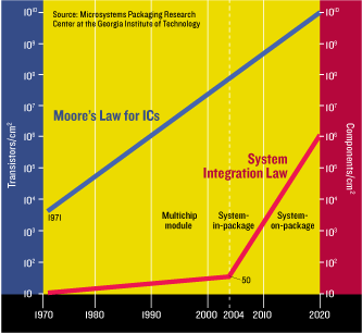
Growing Faster: System integration using system-on-package (SOP) technology from Georgia Tech’s Microsystems Packaging Research Center will see “More Than Moore’s Law” take hold, as measured by component density. From about 50 components per square centimeter in 2004, component density will climb to about a million per square centimeter by 2020. Functional system density will escalate similarly.
Squeezing so much into tiny spaces is our mission at Georgia Tech. If we have our way, products will shrink by much more than the factor of 10 typically expected every few years now. Instead, they will shrink by factors of many hundreds and even thousands in the same time frame.
We began this research in 1993 with a proposal to the U.S. National Science Foundation for an Engineering Research Center, which the NSF then funded. Today we are not alone in this endeavor: researchers around the world are using SOP to combine diverse technologies in new, unusual, and cost-effective ways. Everyone is after ultracompact products built with any combination of digital, analog, radio-frequency, and even optical circuitry, as well as a variety of sensors.
For more than 40 years, circuit designers have counted on the steady increase in transistor density in their pursuit of convergence. For example, engineers at Texas Instruments are building entire signal-processing subsystems with diverse functions on a chip of silicon—a system-on-chip, or SOC, as it’s called. Designing such a chip has its technical problems, too, particularly if digital logic and memory for computation must be combined with analog and RF communications circuitry. Usually, these dissimilar circuits not only operate at different voltages but also require different processing steps during manufacture. Complicating matters further, analog and RF circuits must be electrically isolated from digital ones. Design time and complexity, along with fabrication costs and time to market, can skyrocket.
At Georgia Tech we take advantage of package integration. We eliminate the individual passive component packages—the hard black tiles you see on the large system board inside your PC, DVD player, or cellphone. Those packages measure anywhere from a quarter of a millimeter to as large as 3 cm on a side and a millimeter or two high. Instead of using them, we convert the passive elements to bare, thin-film components only micrometers thick and embed them in our multilayered system package. Such thin-film components are anywhere from a thousandth to a millionth of their original packaged size. Further, in our latest research, we have eliminated bulky IC packages, too, by embedding their bare chips in the SOP package. We even shave the chips down to a thickness of 25 micrometers, from their original 1 millimeter.
SOP does away with the bulky system board and makes the package the centerpiece of system integration. Highly integrated, this multilayered package holds all the parts—thinned, bare IC chips; passive thin-film components; and wiring and interconnections.
The result is that we raise the component count—and the number of functions—per unit volume well beyond what is possible by ignoring the package and simply relying on Moore’s Law for ICs. But smaller size is not the only benefit. Size reduction also allows for much faster chip-to-chip signals at lower currents and voltages—which cuts power dissipation.
ICs and discrete components are combined in such a small package that, eventually, handhelds will become megafunction devices
Note, too, that with SOP we’re not limited to silicon or any particular technology; we can use whatever we wish. Another benefit is that we don’t force dissimilar technologies to cohabit on a single piece of silicon, as may happen in an SOC design that tries to put many functions on a single IC chip.
We use devices made of silicon, gallium arsenide, or silicon germanium—whatever material is best suited for our ICs and discrete components [again, see “ ”]. For example, we use silicon ICs for digital circuits and some RF devices, such as amplifiers and oscillators. In the package, we embed antennas, capacitors, inductors, resistors, filters, crystals, and waveguides. We embed these parts as thin films in the layers of the package. For biosensing applications, we form sensors of tiny resonators, nanotubes, nanobelts, and microelectromechanical systems (MEMS). And when quantum and molecular devices become available, we’ll be able to use them, too.
Because we’re not forced to use any particular technology, the time it takes to design and fabricate a system is much shorter than before, and time to market is shorter as well. Further, the circuitry and package of an SOP-based system are designed and fabricated in parallel—not serially, one after another—which saves time and money.
We need not compromise speed, cost, time to market, or reliability. Such compromises must be made when dissimilar technologies are combined in a single IC. Yet our SOP with its many functions will be no bigger than the bulky package of an SOC, which cannot combine nearly as many technologies as we can. Our SOP can even provide cost-effective chip-to-chip optoelectronics, replacing copper wire with optical fiber, and can include miniature waveguides, gratings, lasers, and detectors.
To build an SOP for, say, a mixed-signal, multifunction system, we can fabricate multiple system functions on a single substrate. We start with an ultrathin yet stiff composite substrate. Next we deposit layers of dielectrics and conductors as well as the thin-film components, including capacitors, resistors, inductors, filters, switches, and waveguides. But unlike a silicon wafer, which is round, our SOP wafer is square, measuring, so far, 300 mm on a side. Completed wafers are electrically tested and diced into square or rectangular system packages measuring anywhere from 1 to 2.5 cm on a side. Some ICs of silicon or gallium arsenide or other material—whether meant for processors or memory—can be connected to the top surface of the SOP with ordinary lead-free solder or copper interconnects.
Our SOP concept goes well beyond merely placing multiple chips in a package, as IBM did some 20 years ago in its ceramic multichip module. Until our SOP came along, IBM’s MCM was the most highly integrated package in existence, with copper wiring for interconnecting ICs. But it has no embedded thin-film components as does an SOP, and it requires a system board. Thus, while an SOP attacks the 90 percent part of the system problem, an MCM does not.
SOP is also different from a system-in-package (SIP), another miniaturization technique being deployed by most IC, package, and cellphone companies. In the SIP approach, bare or packaged IC chips are stacked on top of each other in a three-dimensional arrangement. But SIPs address only 10 percent of the system problem and ignore the problem of bulky passive components. An MCM or an SIP must still plug into a traditional system board.
Our SOP has many advantages over those other approaches. Perhaps the biggest benefits are that, in a cellphone, for example, we have none of those 400 passive components to assemble, and there is no system board, since the board becomes the package. And the package can hold silicon digital ICs alongside ICs made of other materials. Such capability is next to impossible for an SOC and has not been demonstrated for an SIP.
Because an SOP uses separate chips for its different functions, designs are simpler and manufacturing time shorter than for an SOC. And for computing applications we can even remove the space-eating and high-resistance wires on the ICs that distribute clock and power. Instead, we put those wires in our package. We can also move nanoscale wiring that is on chip into the package. There, such wires can be wider and thicker than what can be reasonably fabricated on chip; wire resistance is lower, improving speed and reducing the energy lost to heat.
An SOP design relies on many thin horizontal layers of dielectrics holding conductors and components. For computing applications, we deposit multiple layers of ultra-low-loss and ultra-low-dielectric-constant insulators along with electroplated copper interconnects made of 2- to 5-mm-wide copper traces. The insulators are made of conventional polymers, such as epoxies, or more advanced polymers, such as polyimide or benzocyclobutene, that have outstanding dielectric properties.
We also embed 1-µm-thick decoupling capacitors very close to each IC chip to minimize power noise. To accomplish this, we invented novel ceramic decoupling capacitors that can be processed at relatively low temperatures. Traditionally, ceramics have the highest dielectric constant and lowest dielectric loss, compared, for example, with organic materials. Ceramics’ drawback is that the capacitors must be fabricated at very high temperatures, well beyond what is typical of electronics fabrication. Capacitors made of organic materials, on the other hand, can be fabricated at lower temperatures but suffer from very low dielectric constants. We developed capacitors with ceramiclike properties but fabricated at the temperatures used for organic materials in an advanced low-temperature chemical process referred to as a hydrothermal process.
For RF applications, we form organic-compatible thin-film capacitors that are stable because of their low temperature coefficient of capacitance. We also fabricate high-value resistors that are stable because they have a low temperature coefficient of resistance. We form high-quality-factor inductors far superior to any fabricated on silicon. We use a variety of both thin-film and composite technologies to achieve these properties. Thin-film fabrication processes include sputtering, electroplating, and sol gel, as well as the hydrothermal process.
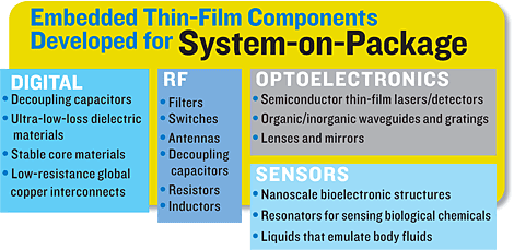
For optical applications, we deposit thin films to form waveguides, optical gratings, mirrors, and lenses. For sensing biological functions in the body, we have developed silicon, zinc oxide, and carbon nanotube sensors that selectively detect the chemicals of body fluids. [See chart, "Embedded Thin-Film Components Developed for System-on-Package."]
We have also built numerous research vehicles that combine RF, digital, and optical functions. The Intelligent Network Communicator was the first such mixed-signal SOP, designed and built at the Microsystems Packaging Research Center in 2003. We used it to learn how to simultaneously design, develop, and optimize our materials and processes. It was a 75- by 50-mm multilayer sandwich, 1.2 mm thick, made of thin-film materials and embedded active and passive components and active devices in packages on the top surface.
We built it to transmit a high-speed digital signal on an RF carrier over an optical channel to help us understand the design and interface issues inherent in combining these technologies. The unit consists of a field-programmable-gate-array (FPGA) IC for the transmitter and another for the receiver.
Each IC supports 16 channels, each with a speed of 155 megabits per second. The transmitter output is multiplexed to generate a 2.4-gigabit-per-second digital data rate that modulates a 5.8â’’gigahertz RF carrier. The modulated signal is transferred to the optical circuitry, which consists of a bare laser diode, waveguide, and photodetector.
The laser diode converts the signals, which are then transmitted as light through the waveguide to the photodetector. Converted at the photodetector, electrical signals return to the analog section, where they are converted back into a digital data stream and received by the FPGA. In the digital section the data are compared with the original transmitted data. The streams should be identical.
The measured waveforms on the module surpassed the design goals, indicating the robustness of our process. For example, the digital block was designed for a 2.4-Gb/s digital data rate, but we found we could send a data stream at up to 3.1 Gb/s. Similarly, the optical waveguide supported a 10-Gb/s data rate with minimal degradation.
The eight thin-film layers of the communicator system board include four dielectric layers holding copper interconnects. Wiring patterns are produced on different layers with advanced photolithographic printed-wiring techniques. Microvias connect the buried wires to digital and RF circuitry both within the package and to ICs on the surface. Thin-film capacitors deposited on one of the board’s wiring layers act as decoupling capacitors to suppress power noise. With our techniques, we routinely achieved densities of 400 components per square centimeter, a figure recently improved to 600–1000/cm2. We expect to reach 10 000/cm2 within a decade. Until recently, the component density of electronic systems on conventional circuit boards stood at about 50–100/cm2.
Since we began developing the SOP concept in 1993, we have worked with more than 100 electronics companies from the United States, Japan, Korea, and Europe. Included are Advanced Micro Devices, Asahi, Ericsson, Ford, Hitachi, IBM, Intel, Matsushita, Motorola, NEC, Nokia, Samsung, Sony, and Texas Instruments. In addition, more than 70 researchers have come as visiting engineers to our center to study SOP and its application to their diverse requirements.
So far, at least 50 companies have taken parts of our technology and applied them to their automotive, computer, consumer, military, and wireless applications. We have also built a number of test vehicles for different companies focused on integrating different combinations of analog, digital, RF, optical, and sensor components in a single package.
Motorola, for example, which was one of the Packaging Research Center’s founding partners, uses parts of SOP technology in two models of its GSM/General Packet Radio Service quad-band cellphones to gain about a 40 percent reduction in board area. The module contains all the critical cellphone functions: RF processing, base-band signal processing, power management, and audio and memory sections. Not only does the module free up space for new features, it is also the base around which new cellphones with different shapes and features (camera or Bluetooth, for instance) can be rapidly designed. Motorola calls its package a system-on-module (SOM), for which it developed its own custom embedded-capacitor technology. It reports it has shipped more than 20 million SOM-based phones.
SOP research is flourishing around the world. At the Institute of Microelectronics in Singapore, for example, Mahadevan Iyer and his co-workers have built an optoelectronic SOP intended for high-speed communications between a network and a home or office. The approach is slightly different from ours, with optical circuits made of silicon. The system transmitted data at 1 GHz. Someday such a device might operate at hundreds of gigabits per second.
At the Interuniversity Microelectronics Center, in Leuven, Belgium, Robert Mertens and colleagues are studying the best type of RF antenna to build in an SOP for a range of wireless communications products yet to be introduced.
At the University of Arkansas, in Fayetteville, Len Schaper and Richard K. Ulrich developed techniques for burying capacitors, resistors, and inductors in the layers of their SOP board. They determined that almost all the resistance and much of the capacitance needed for a system can be embedded in the board using vacuum-deposition processes typical of the IC industry.
At the Royal Institute of Technology, in Stockholm, Sweden, Hannu Tenhunen and his group are comparing the cost of an SOP to the cost of an SOC-based system to better understand SOP’s cost advantages. And at Georgia Tech we have applied innovative and low-cost chemical processes to form more than 20 thin-film digital, RF, optical, and sensor components for SOPs. Included are embedded capacitors in the microfarad range, up from the nanofarad, where they had been.
The next step for SOP is to add optical signaling between chips inside the package by sending light signals through built-in optical waveguides. This way, a microprocessor will be able to exchange data with a memory chip at processor clock rates, rather than at the few hundred megahertz possible now.
The main problem with optoelectronics has not been performance but high cost. However, we can reduce cost by building SOPs in batches. For example, as is done for ICs, hundreds of small optoelectronic SOPs could be fabricated on a single large board of 400 by 500 mm. Individual packages measuring, say, 25 mm on a side could then be cut from the board much as individual dies are cut from a large silicon wafer.
In addition to waveguides, we have built complete thin-film, chip-to-chip optoelectronic systems that include lasers, optical gratings for selecting specific wavelengths, microlenses for focusing light onto gratings, and photodetectors. Most of the structures have been made with light-sensitive polymers and lithographic techniques similar to those used to make ICs.
Three developments are needed, however, if the SOP concept is to succeed on a large scale. First, design tools must be developed for the simultaneous design of digital, analog, and optical circuits along with the package. Although tools exist for designing individual digital and analog circuits and for boards themselves, none exist for designing a whole system like ours. Georgia Tech is setting up an industry consortium to focus on developing such tools. And to push SOP to the next generation, we are also arranging several industry consortia on embedded active and passive components, mixed signal testing, nanometer materials and packaging, and thermal material interfaces, among others.
The second development that’s needed would be a change in today’s IC- and system-package manufacturing. Today, semiconductor companies design and fabricate ICs but usually rely on outside companies for their packages. System companies design their systems while counting on packaged ICs from semiconductor companies, system boards from board companies, and the assembly of the entire system by contract manufacturers. But because of the way an SOP is designed and integrated, it must be developed for fabrication at the same time. The manufacturing model will therefore have to change if the SOP method is ever to become mainstream.
The third change needed deals with process technologies. SOP substrates are a hybrid: they need a clean room like those for ICs, thin-film processes along with low-cost, large-area board processes. Accordingly, a number of different manufacturing techniques for SOPs are emerging, including an SOP-like package with thin-film deposition on silicon wafers by Philips; organic boards by Shinko, Ibiden, and Matsushita; and ceramic boards by Murata and TDK.
At Georgia Tech we believe that the market for multifunctional products and the advantages of designing chips and system packages concurrently are so compelling that companies will just have to design and fabricate everything together. And as the SOP concept takes off, design-tool and fabrication houses will turn their attention to developing powerful programs for concurrent design and advanced manufacturing, just as they did in the past decade when the SOC was in its infancy.
Acknowledgment: The author wishes to thank his Georgia Tech team of faculty, engineers, students, and representatives from industry for their contributions included in this article, and both the Georgia Research Alliance and the National Science Foundation—Engineering Research Centers for their funding of SOP technology for more than a decade.
About the Author
RAO R. TUMMALA, an IEEE Fellow, is a member of the National Academy of Engineering and is the Pettit Chair Professor in Microsystems Packaging at the Georgia Institute of Technology, in Atlanta. He is also the founding director of the Microsystems Packaging Research Center, one of the U.S. National Science Foundation’s 22 Engineering Research Centers. Before joining the Georgia Tech faculty, he was an IBM Fellow and director of the company’s Advanced Packaging Technology Laboratory.
To Probe Further
The May 2004 IEEE Transactions on Advanced Packaging was devoted to system-on-package research. See R. Tummala et al., “SOP for Miniaturized Mixed-Signal Computing, Communication, and Consumer Systems of the Next Decade,” pp. 250–267, and R. Tummala, “SOP: What It Is and Why?” pp. 241–249.
Another article describing a high-speed wireless device, by R. Tummala and J. Laskar, “Gigabit wireless: system-on-package technology,” is in Proceedings of the IEEE, Vol. 92, 2004, pp. 376–387.
“Packages Go Vertical,” IEEE Spectrum, August 2001, describes system-in-package technology. "Chips Go Vertical," Spectrum, March 2004, looks at methods for stacking chips.


