Originally published May 1996
The dream of building machines that mimic the behavior of animals and people dates to the dawn of technology. With the advent of cheap and powerful digital computers, that dream is becoming reality. Computers, though, struggle hard to process the type of visual input people can instantly absorb, as when we identify a familiar face, read a scrawl, or hit a hurtling tennis ball. One reason for the contrast is that visual images contain so much information: a 1-second-long, uncompressed NTSC video segment amounts to about 22 MB of data. The need to process, store, and ship such vast data streams is what hampers machine vision. Yet miracles of real-time visual behavior are performed by the common house fly, whose brain is the size of a grain of rice. Clearly there is much to learn from the computational strategies of the nervous system.
For a decade now, research at many university laboratories has sought to understand the biological circuits and principles that underlie vision and vision-based behavior in flies, frogs, cats, monkeys, and human beings. At the same time, the complexity of the circuitry a single silicon chip can support has reached new heights. Capitalizing on these gains, a few researchers have built electronic chips that mimic neurobiological circuits related to visual processing: so-called neuromorphic integrated circuits, a term coined by Carver Mead at the California Institute of Technology (Caltech), in Pasadena. A neuromorphic imaging sensor consists of arrays of photoreceptors combined with analog circuitry at each picture element (pixel) in such a way as to emulate the vertebrate retina. More specifically, the sensor, like the retina, can adapt locally to vast changes in brightness, can detect edges, can signal temporal changes, and can detect motion [Fig. 1].
Until recently, vision chips of this kind were laboratory curiosities. Now, they are powerful enough for use in a variety of products. In the long term, the principles of neuromorphic design will enable machines to interact with the environment and with persons, not through keyboards or magnetic-strip cards, but with the help of robust, cheap, small, and real-time sensory systems of the type that have been ubiquitous for the past 400 million years. Appliances will become life-like: smart doors will let us pass once they have seen our faces; cars will navigate by themselves; and roach-like cleaners will scurry along floors to remove dust and dirt. Last but not least, because of their similarity to biological nervous systems, neuromorphic systems can provide a "natural" substitute for damaged parts of the human nervous system, such as the retina or parts of the cerebral cortex.
Unconventional sensors
Functionally, neuromorphic vision chips do what a video camera does when combined with a computer running some dedicated vision program, perhaps an algorithm for detecting edges. Computationally, though, the architectures of the two systems are quite different. Neuromorphic systems, like nervous systems, use massively parallel, analog, nonclocked, collective processing, rather than the numerical and symbolic processing basic to artificial intelligence and conventional machine vision. These desirable neuromorphic properties can implement types of mathematical operations that occur in early vision, as it is called. (Early vision is the set of processes that make use of two-dimensional intensity arrays to recover distance, texture, and other physical properties associated with the surfaces of the three-dimensional objects visible around the viewer.)
The first reflex of today's system engineers, surrounded as they are by digital computers, is to sample and digitize the incoming video signal as soon as possible. Yet since the brightness of an image is continuous in time and amplitude, why import unnecessary artifacts? Why not instead exploit the physics of conductances, capacitances, and nonlinearities inherent in transistors to implement operations that are expensive in the digital domain? When such analog circuits are integrated with 2-D arrays of photoreceptors, the resulting silicon retinas capture the image with a virtuosity no digital computer can match unless capable of hundreds of millions of floating-point operations per second. And the package can be as small as 1 cm2.
Before these devices can be built, several key components must be designed. Adaptive photoreceptors are needed to sense image intensities over eight orders of magnitude--the range of natural lighting from moonlight to high noon. Linear and nonlinear resistive grids must filter the image in order to reduce the ever-present noise and to enhance and detect certain features, such as edges. Smart communication protocols are necessary to send streams of visual information between chips. Velocity sensors have to reliably detect motion in the scene. Finally the chips must be able to adapt their outputs to wide variations in parameters using on-chip learning.
Not every IC dedicated to visual algorithms is a neuromorphic vision chip. The latter processes the image on the same physical plane as it acquires the image (focal plane processing). On the other hand, dedicated signal-processing circuits take the digitized output of a camera and apply a particular visual algorithm to every picture element (pixel) in the image, one after the other.
The dedicated circuits are usually based either on standard digital signal-processing (DSP) chips or on digital systems specially designed for such applications as block matching for video applications or filtering images using convolution. Block matching is popular for estimating motion in images. In convolution, the most common image-processing technique, passing a "filter function" over each point in the original image transforms it into the filtered image. The new value of a pixel is the sum of the products of this filter function with the image intensity at each pixel, suitably normalized.
In these applications, a mathematical operation that needs to be repeated over and over again is cast in special-purpose digital hardware; otherwise, it would limit system performance too much. One example is the correlation chip that Woodward Yang at Harvard University, Cambridge, Mass., developed for recognizing faces. Here, the most demanding operation is to match one face against a large database. So small chunks of the image are fed to Yang's digital chip, which matches them against a template. The chip carries out about 100 000 correlations each second on a 64-by-64-pixel image and outputs the best fit. But although the correlator chip by itself only requires 0.1 W of power, the entire system, including camera and microprocessor, is still large and power hungry.
Adaptive photoreceptors
Today, there are two approaches to image acquisition. The first, sensors based on charge-coupled devices (CCDs), dominates the consumer market. The CCDs sense light intensity by integrating the photocharge in time on a grid of some 800 by 600 pixels. The continuously valued output at each pixel, digitized in time, constitutes the output of the camera. It is typically sent to a "frame-grabber" board, where its amplitude is digitized (usually to 8-bit, or 256-level, resolution) for further analysis.
The amplitude of light in the natural world, however, swings over eight orders of magnitude from moonlight to a sun-filled day, while the dynamic range of CCDs is unfortunately much less. When the dynamic range needed to process the image exceeds the CCD's capability, the image is clipped; and blooming can occur when the charge on a pixel exceeds its holding capacity and the excess spills over into neighboring pixels. A clipped region in the image will be uniformly white, with no details apparent. Blooming manifests itself by a white line in the image, created by the excess charge that flows from the bright pixel onto and along a rail in the imager. The usual remedy for a limited dynamic range is to include automatic gain control. In this case, a mechanical iris will serve, or else the charge integration time of the imager may be adjusted to the brightness of the scene.
CCD cameras do not compute. Indeed, they should not, since their output, a series of bits that can easily be transmitted to a TV monitor, should look as much as possible like the input when displayed on the screen. This also implies that the image requires high resolution all over, since it is not known ahead of time where the viewer will be looking.
Biological creatures view things differently--the photoreceptors in their eyes sense the intensity continuously in time and adapt to the local image intensity in both space and time, thereby maximizing the receptors' dynamic range. Photoreceptors with similar properties can be built using CMOS devices. A simple photodiode can logarithmically compress the photocurrent into a voltage signal, but its response is very slow at lower intensities. Further, device mismatches due to fabrication variables will skew the response of adjacent receptors to identical input. Indeed, variation in voltage due to device mismatch can be as large as the signal itself. All these problems can be solved by adaptive photoreceptors.
Some of the best adaptive photoreceptors have been designed by Tobias Delbruck at Caltech. The response of his five-transistor photoreceptor is logarithmic, so that the differential response to a constant contrast is unaffected by changes in the absolute light intensity. Its output adapts to slow (seconds long) changes in image intensity over more than six orders of magnitude, while preserving a high gain for transient changes in the image. And, in stark contrast to CCDs, no expensive clocks are needed, reducing power consumption and the need for support circuitry.
There is a price, though. In a 1.2-um CMOS process, a single adaptive photoreceptor uses about 52 by 52 um2 of silicon real-estate, compared to 7 by 7 um2 for a state-of-the-art CCD pixel [see "Vision chips compared"].
Image resolution is another important difference between artificial and natural vision systems. While we primates sample the world in daylight using one to two million photoreceptors, other animals need many fewer. Highly evolved insects that use vision to find food and mates and avoid predators and obstacles have in effect 10 000 or fewer pixels with which to sample their environment. Although their visual performance in real time is beyond current machine-vision systems, even the cheapest hand-held video camera has many, many more pixels. The moral here is that while we humans are used to seeing high-resolution images, many visual tasks need far fewer pixels.
Local computation with resistive grids
In the "living" retina, the output of the photoreceptors is fed into a tightly interconnected network of cells that spreads the signal horizontally within the retina [see "cellular neural network"]. A kindred strategy has been adopted in many neuromorphic vision chips, where the photoreceptor outputs are fed into a 2-D square or hexagonal resistive grid.
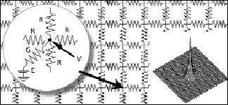
Resistive networks are an essential part of the neuromorphic engineer's repertoire, because they implement particular filtering operations. Assume, for instance, that the values of the batteries, E, attached to one node in a rectangular resistive grid [Fig. 2] are proportional to (actual or logarithmically compressed) image intensity at this location. Then the voltage, V, at each node of the network can be considered to be an average resulting from the current between battery and node and the currents across all four horizontal resistances, R, connecting the node to its neighbors. Decreasing R increases the current within the grid, leading to more averaging (smoothing). Increasing R or, conversely, increasing the conductance G that links the input to the network, has the opposite effect of coupling V closer to the battery, resulting in less smoothing. At steady state, the mathematical relationship between the input E and the output V (the voltage in the grid) can be expressed by convolving or filtering the input with a filter function that depends on the exact network configuration and on R and G [Fig. 2, inset]. The degree of smoothing or low-pass filtering is determined by the product of R and G.
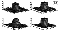
The filtering properties of an analog very large-scale integration (VLSI) resistive grid are demonstrated in Fig. 3. Because the parasitic capacitances are small, the steady-state voltage distribution is reached in less than 5 us--one key advantage of analog computation for early vision. The theoretical insights on how to use resistive grids in early vision processes were pioneered at the Massachusetts Institute of Technology (MIT), Cambridge, by Berthold Horn, Tomaso Poggio, and one of us (Koch).
Implementing filtering by means of convolution on a digital computer is straightforward but can be expensive. The spatial extent, the region over which the filter function is non-zero, is called its support and is expressed in pixels, m. (The Fig. 2 filter's support is about seven pixels.) Implementing the 2-D filters used in early vision algorithms on a digital processor requires 4m additions, multiplications, or divisions per pixel. Thus, the total computational cost of filtering grows linearly with the number of pixels, rendering most early vision algorithms expensive in terms of machine cycles. This becomes particularly painful when using larger filters--that is, with more blurring. Blurring a single 1000-by-1000-pixel picture with a 2-D filter that is 11 pixels across takes about 44 million operations. In analog hardware, conversely, implementing a large filter can be done by simply adjusting R or G. The convergence time of the resistive net depends only weakly on image size.
Interestingly, using resistances and batteries to compute would not have been news to engineers in the 1940s and '50s. At the time, digital computers were still too cumbersome for many practical problems, and engineers resorted to analog computers that occupied entire rooms. Today, analog computers are making a limited comeback, allowing applications that require much computation to be carried out in a highly parallel manner on a single chip.
Early vision algorithms must be able to smooth over surfaces; but they must also detect discontinuities in the image and prevent smoothing from occurring there. This capability, called segmentation or nonlinear, data-dependent smoothing, comes naturally to resistive nets. In the early '80s, many vision algorithms were introduced that used a binary variable, termed a line process, to represent discontinuities in color, motion, texture, or depth (surfaces at different distances from the imaging system).
In its simplest form, nonlinear smoothing assumes that if the depth (or color or motion) of two neighboring locations is very similar (that is, if the difference between the two is below some threshold), both pixels represent a portion of a scene lying on the same surface out there in the world and should have the same depth. Therefore, any difference between the two locations is due to noise and should be reduced by smoothing. Conversely, if the difference between the depth at neighboring pixels is above some threshold, presumably the two pixels are lying on two planes of different depths (in this example). The implication is that a discontinuity has been detected that would be smeared if averaging were used to smooth the image.
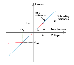
These high-level constraints have been embodied in a two-terminal multitransistor device, termed a resistive fuse by its inventor, John Harris, now at the University of Florida, Gainsville. If the voltage across the device is small, it acts like a resistance, conducting a current proportional to the voltage gradient. If the voltage gradient is above a threshold, the fuse kicks in and the current drops to zero, preventing any smoothing [Fig. 4]. These devices can be added at little cost to every node in the resistive grid, substantially enhancing performance.
The cellular neural network (CNN) chip is another way of using analog hardware to implement such image-processing operations as smoothing and discontinuity detection. Its chief advantage over a resistive net is that it can be programmed to carry out a wide range of local mathematical operations. This flexibility comes at a price, though, for the basic pixel is very large, and the chip, while very fast is quite power hungry.
Retinal processing
The ability to detect the existence and location of edges and other marked image features is a key virtue of biological visual systems. Resistive networks can do the same if at each pixel, the electric current across the conductance G is read out in place of the voltage V. The current will be large if a node's input voltage is very different from the average voltage of the network, and close to zero if the input varies little from the network average. Thus, the new configuration serves as a high-pass filter that will sharpen abrupt changes such as edges. This is the main idea behind the silicon retina, pioneered by Carver Mead and Misha Mahowald at Caltech.
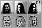
In the silicon retina, a logarithmic photoreceptor appears at each location (in place of the battery of the last example), and the output is a high-pass-filtered version of the input image, with enhanced edges. The retina also performs local, spatial adaptation since it will always signal a deviation of any one pixel from its neighbors. A more highly evolved version of this retina has been built by Kwabena Boahen at Caltech and Andreas Andreou at Johns Hopkins University, Baltimore, Md. The silicon retina follows design principles of the vertebrate retina, in that it sets the local gain to be inversely proportional to the local image intensity, yielding an output proportional to the local contrast. Add in the spatio-temporal bandpass filtering also implemented by this circuit, and its output enhances features in shadow as well as those awash in bright sunlight. As readers can judge for themselves, the output of a CCD camera lacks the dynamic range to represent the image's dark and bright portions simultaneously [Fig. 1, top]. In this case, a face recognition system is more likely to succeed if a silicon retina serves as the front end [Fig. 1, bottom].
Granted, the resolution of such retinas (at present 210 by 230 pixels) is less than for CCD cameras. Still, their very fast temporal response, on the order of a few microseconds, plus their performance, absence of complex clocking circuitry, and low-power (50 mW) requirements, make them candidates for many everyday applications. Face or fingerprint recognition systems at the doors of homes and at the automatic teller machines of banks are obvious examples.
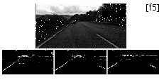
The outlier detection chip is a specialized design for finding points in the image that differ in intensity from their neighbors. It is an industrial-strength neuromorphic vision chip that uses a variant of the resistive fuse. It locates edges in its photoreceptor array and outputs them at frame rates (for a TV or consumer camera, usually 30 Hz) to a digital circuit for further processing. One possible use is to locate lane markings on a road [Fig. 5].
In Germany, a government-sponsored program is under way to bring similar circuits into products. It includes a Daimler-Benz AG-led effort to develop vision sensors for use on automobiles. In the fall of 1994, the company's research labs succeeded in getting a Mercedes station wagon, filled to the brim with digital electronics and equipped with eight CCD cameras, to drive itself from Stuttgart to Paris--no mean feat. Neuromorphic concepts will be used to condense the systems of electronics and cameras into a tiny package that will allow such driver-assistance systems to find large-scale applications in the consumer market.
Communicating with spikes
The communication principle most used in the central nervous system is asynchronous pulse coding to share the results among neurons. Can this strategy be used in vision chips?
The output of any photoreceptor array is scanned out serially (usually called raster scanning). That is, the entire image is read out every so often and needs to be processed no matter whether anything of interest happened in the interval. Thus, each pixel in the image is accorded some fixed fraction of the total communication and processing bandwidth. But most of the time, nothing much happens at most locations in any scene. A more intelligent strategy would be to send out a signal only when an event has occurred--the approach taken in most parts of the brain.
Multichip systems based on such asynchronous communication protocols have been designed by a number of researchers, in particular Eric Vittoz of the Swiss Center for Electronics and Microtechnology Inc., Neuchatel; Mass Sivilotti of Tanner Research Inc., Pasadena, Calif.; Misha Mahowald and Rodney Douglas of Zurich's Eidgenossische Technische Hochschule; Paul Mueller of the University of Pennsylvania, Philadelphia; John Lazarro of the University of California, Berkeley; and Kwabena Boahen of Caltech. In their systems, individual pixels generate a pulse (or spike, in the language of neurobiology) that is assigned a unique address and placed on a bus. The chip that receives the retina's output now knows that something of interest happened at that address in the retina. Additional circuitry is needed for arbitration when multiple events have been generated at the same time.
Compared to conventional raster-scan communication techniques, "address-event" communication protocols make much fuller use of the available bandwidth, because only relevant data are transmitted. In fact, the most efficient way to use a channel of this kind is to transmit only information that signals a deviation, in space or time, from some average activity. Further, because spikes are reported asynchronously, and not in synchrony with a clock, their timing can yield valuable information about the timing of events in the outside world. Spike coding does, however, require that both the sending and the receiving systems be able to communicate asynchronously.
Address-event communication protocols will be needed when it comes to replacing the optic nerve that leaves the retina and in humans contains a million fibers. Chips cannot be built with more than a few hundred output wires, and the output of a wired optic nerve must talk to neurons that receive spikes as inputs. It therefore makes sense to convert the output of a prosthetic silicon retina into pulses for further processing by the brain.
Estimating motion
To summarize, it is now possible to build ICs that capture the image in an adaptive manner and filter it to enhance features such as edges. In the real world, however, either the sensor or objects in its environment (or both) move, sometimes quite rapidly. Thus, the next (computationally expensive) step is to detect motion throughout the image by estimating the optical flow field associated with it; this field is the output of a vision algorithm or circuit that assigns a vector to every location in an image, to indicate in what direction the image intensities have moved during the preceding interval.
While in principle many types of sensors can detect motion, they have serious drawbacks. For example, radar flounders in a cluttered environment, while a gyroscope can identify only its own motion. Vision chips, on the other hand, promise to estimate their own motion as well as that of other objects throughout the field of view, and may do it in a single step, at a low cost, and without revealing their presence--a great asset in an age of "stealth" technologies.
The output of a velocity vision chip is the optical flow field. Used correctly, it can estimate when the sensor will collide with an approaching object, such as a car, and in what direction the sensor is moving, and it can alert its user to other moving objects in the scene (for example, an intruder). Given the usefulness of the optical flow field, the design of robust, analog velocity sensors is a thriving area of research. Standard computer vision methods rely on the evaluation of ratios of spatial and temporal derivatives of the image intensity and thus do not lend themselves to analog implementation, which lacks the high numerical accuracy required.
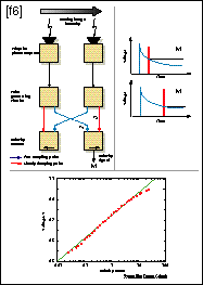
The problem is to build a sensor that unambiguously signals velocity, independent of the level of brightness of the background and the contrast in the stimulus, and over a wide range of speed. The feat has been accomplished by Rahul Sarpeshkar and Jorg Kramer at Caltech. Their circuit works by detecting an "event" in the image at one pixel and by timing how long the event takes to propagate to an adjacent pixel. Suppose this event is an abrupt increase or decrease in the image intensity [Fig. 6]. Its detection at one pixel triggers a slowly decaying signal (generated by a nonlinear filter with a changing time constant). Then the detection of an event at the neighboring pixel, presumably due to the movement of the same image feature to a new position, generates a fast pulse, which samples the slowly decaying one. The amplitude of the sampled voltage signal indicates the speed with which the event moved between the two pixels.
The form of the decaying voltage pulse [P1 in the top left portion of Fig. 6] produces a logarithmic dependency of the output voltage on the image velocity over at least three orders of magnitude. Performing an equivalent digital algorithm would require about 50 operations at each pixel (assuming the image is shifted by five pixels in either direction and that accurate sub-pixel interpolation is possible) [see "Vision chips compared"], which adds up to a lot when analyzing motion in large images. Further, in the analog device, the output signal of the velocity sensor degrades gracefully with contrast, while always maintaining direction-selectivity.
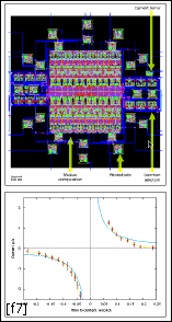
Because of their compact nature, velocity sensors can form very dense arrays (for instance, 128 by 128 pixels designed in a 0.7-um CMOS process). This density is more than adequate for an evaluation of notable features of the optical flow across the entire image in real time. One feature involves estimating how long some object, approaching at a constant velocity, will take to crash into the observer. Computing this time-to-contact requires only the integration of the output of velocity sensors arranged on a closed contour, such as a circle [Fig. 7]. A single low-cost sensor with its on-board photoreceptor array can help cars or robots avoid crashes. And all of this on a few square millimeters of silicon!
Other optical flow chips are being designed to estimate the direction of heading and to pinpoint any discontinuity in the optical flow, whether it indicates a looming car, an intruder in the garden, or an approaching missile. But further development is required before velocity sensor chips can spread into commercial and military products. For one thing, the sensor of Fig. 6 estimates velocity between only two points; whereas it is necessary to integrate the output of a number of suitably weighted sensors distributed over patches of the image to obtain the 2-D optical flow field. Also, because the motion-processing cell is itself so large, it makes sense to build a retina chip on which the image is acquired and the events detected that trigger pulses on a retina chip. These asynchronous pulses are then sent to a second chip, by means of the address-event communication scheme discussed above, where the actual motion field analysis occurs.
Learning systems
All this praise notwithstanding, the fact is that analog CMOS circuits are less than accurate--particularly in the subthreshold-voltage regime in which they usually operate. Voltage offsets of 20 mV are routinely observed in most analog chips and would matter little for a logical 0 and a 1 differing by some volts. But the presence of such offsets throughout the analog circuitry plagues the circuit designer. Nature again provides inspiration.
Architecturally, a salient difference between brains and computers lies in their use of memory. Following the design laid down by von Neumann 40 years ago, the storage of data is distinct from the computations occurring in the central processing unit. Not so in brains. Adaptation and learning occur at every level of the nervous system, from the retina to the highest region of the cortex, and are intermixed with processing circuitry. Apparently, no neuronal element is used exclusively for either learning or computation.
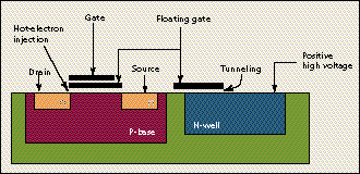
Some uses of adaptation are evident in the adaptive retinas presented already. But the lesson from neurobiology is that adaptation (conceptually akin to learning) should occur at every level of processing. To this end, floating-gate technology (as used in erasable programmable ROM digital memory) has been brought to the point where it can routinely be used to perform local, synapse-like learning. It was Lance Glasser at MIT in 1985 who first showed how to selectively store a 0 or 1 in a floating-gate memory. The floating gate is isolated from its surroundings by thin layers of silicon dioxide, and the electric charge on it is changed in a highly controlled manner. Either of two very different physical processes is used: high-voltage tunneling to remove electrons, or hot-electron injection to add them. In neuromorphic circuits, the concept has been extended by Mead and his students to enable storage of analog information as a varying charge on the floating gate of a transistor [Fig. 8].
Floating-gate transistors, fabricated in standard CMOS technology, can learn the parameters that not only optimize a particular system's performance but may also depend on the environment peculiar to the system. An example is a real-time neuromorphic system that mimics the oculo-motor system found in primates [Fig. 9].
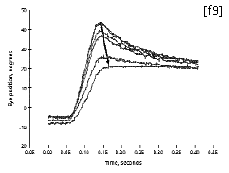
In humans and other primates, if an object suddenly appears on the periphery of the visual field, the eyes visually center it with a swift movement called a saccade. Under certain conditions, saccades undershoot or overshoot their target. In people who have suffered accidents or strokes that impair their eye movements, or in monkeys with experimental lesions, such deficits are often compensated for in a few days. So, too, the neuromorphic system initially displays this suboptimal performance. Then on-chip floating-gate circuits--driven by the error signal from a motion detection chip--correct for the overshoot, iteratively reducing the gain of the initial burst response until the desired response has been achieved. This simple application of learning circuits that are fully integrated into the sensing and computing circuitry only hints at more exciting things to come.
View of the future
Many other advances could be discussed. Silicon retinas are not limited to the region of visible light. One trend in infrared processing is to integrate heat-sensing elements with resistive grids to enhance local contrast. Combined with emergent technologies for room-temperature infrared sensing, this development promises a generation of infrared silicon sensors. A continuous version of discrete resistive grids, akin to a resistive sheet and made out of polymers, might lead to a more compact "plastic retina."
Evidently, highly integrated electronic sensors can utilize lessons gleaned from the way the nervous system works, and in so doing gain significant advantages over CCD cameras and digital computers. With their small size and low power consumption, and with their ability to output spike-like pulses, they are attractive as prosthetic devices for retinal and cortical implants and as "eyes" for the cyborgs of science-fiction fame.
Biological vision systems, honed by several hundred million years of surviving a hostile, real-time environment, employ strategies that are conceptually quite distinct from those used in engineered digital systems. The conceptual rethinking required for designing neuromorphic vision systems seems well worth the effort and should lead to artificial vision systems that are cheap and small and may eventually rival the performance of animals.
About the Authors
Christof Koch (M) is professor of computation and neural systems at the California Institute of Technology, Pasadena. His research focuses on biophysical mechanisms for storing and processing information in single neurons, as well as the computations underlying motion and visual attention in mammalian cortical networks. His laboratory builds smart neuromorphic chips to solve a host of applied vision problems. Together with Nobelist Francis Crick, he works on the neuronal basis of visual awareness and consciousness. His homepage ishttps://www.klab.caltech.edu.
Bimal Mathur (M) is a member of the technical staff at Rockwell International Science Center, Thousand Oaks, Calif. The group he heads develops neuromorphic vision chips for applications in industrial inspection, intelligent vehicles, and military systems. He previously worked on charge-coupled devices and signal processing.
The research reported here was supported by the Office of Naval Research and by the Center for Neuromorphic Systems Engineering of the National Science Foundation. The data shown in Figs. 3 and 5 were obtained by Craig Reinhart at the Rockwell International Science Center.


