The Conversation (0)

This is the digital age. From flashy cell phones, games, PCs, and PDAs to the behind-the-scenes automotive, medical, and Internet components, progress in digital computing owes much to the software that helps designers create and connect millions of transistors. But with the trend toward mixed-signal chips in a communications-centric world, everyone is finding the need for a little bit of analog. As many electronic products get smaller yet do more, designers face special challenges as they add analog circuitry to an otherwise digital chip.
Only recently have analog/mixed-signal designers had any help from electronic design automation (EDA) software. Now the established EDA vendors and a group of start-ups are competing for a share of the growing analog/mixed-signal chip design business. The result is a steady stream of new tools.
Hottest on the list of new EDA offerings are the so-called analog synthesis programs, which offer an automated way to turn specifications into a working component. Unfortunately, they are not as well known as their digital counterparts.
Synthesis, which ushered in the modern age of digital design, lets designers describe circuit functions in terms of software code, rather than with symbols and schematics. This code is then compiled into a list of standard cells, the physical implementation of a logic function. Then, thanks to automated layout, a stable of engineers is no longer needed to place and connect the cells by hand; the computer does the job. With synthesis and automated placement and routing, chip designers can cut design cycle time drastically--digital chip designers, that is.
For analog designers, it's a different story. While digital designers are automating the time-consuming grunt work and focusing on creating more and better electronics, analog designers have been doing things the old-fashioned way--manually. But that situation may be changing.
In fact, growing interest in analog/mixed-signal design was very much apparent at the International Solid-State Circuits Conference in San Francisco last February. Even digital designers packed into sessions on analog and radio frequency circuits, hoping to glean some insights into the integration of high-performance analog and digital components on the same chip.
The Semiconductor Industry Association, San Jose, Calif., predicts that nearly 70 percent of all ICs will have analog components within five years, compared with about 25 percent today. For example, the much-anticipated short-link wireless technologies, like Bluetooth and IEEE 802.11, need an analog interface at the sending and receiving end of every device.
Considering that only 20002500 analog designers are working in North America, according to Gary Smith, an EDA analyst with Dataquest Inc., digital designers might be called upon to learn analog and mixed-signal design skills--attractive commodities in the communications, multimedia, and data storage markets.
Black magic to the rescue
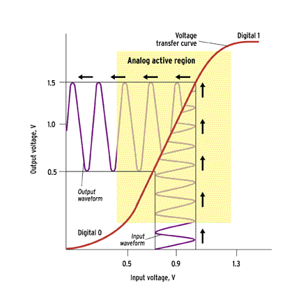
Threading the Needle: Analog design tools must factor in the effect on a device's output voltage of small changes in its input voltage, as shown by the IV curve of an operational amplifier. The steeper the curve, the greater the sensitivity.
Click on the image to enlarge view.
The differences between analog and digital circuits are vast. Digital circuits work by flipping transistors on and off to the states called 1 and 0. They can be described in high-level, hardware description languages (HDLs) and then synthesized into standard cells, which can contain multiplexers/demultiplexers, flip-flops, buffers, and logic gates. Digital circuits have a greater immunity to noise than analog ones because a range of signal values are associated with logical 1 and 0 [see figure]. This noise margin helps to lower performance sensitivity to standard cell placement and routing, making automation of those steps possible.
In contrast, analog circuits work by biasing the transistor somewhere between what the digital world would call fully on and fully off. These circuits don't come in standardized packages; they must be sized and tweaked to work properly. Unlike digital circuits, they cannot yet be described in HDL. Instead analog circuits are characterized more along the lines of "give me an amplifier with a gain of 1000, and make it not burn out." Design automation tools are not yet smart enough to turn that kind of description into a circuit layout. Analog designers manually draw the schematics and connect them so that the transistors stay in the delicate active region. It's no wonder that building great analog circuits is said to involve some amount of black magic.
Because analog designs require skilled craftsmen, who are in short supply, and few parts of the typical analog flow are automated, the average analog circuit takes longer to implement than its usually much larger digital counterpart. Problems multiply if the analog design is destined to be a block on a mixed-signal or system chip. But progress is being made, enough to spark a revolution in EDA for analog/ mixed-signal (AMS) designers, who are now dealing with transistors in the range of millions.
The analog revolution
Granted, it's a slow revolution that relies heavily on designers adopting new design methods. But a handful of companies are moving forward in new areas like analog synthesis and physical layout, and others are improving traditional simulation tools.
"We're on the cusp of a major change in the way people will do AMS design," said Rob Rutenbar, a Carnegie Mellon professor of computer engineering and cofounder of a start-up analog EDA company, Neolinear Inc., also in Pittsburgh. "It's a very cool time to be working on hard-core analog tools. In the 1980s, we were considered lunatics in the wilderness. Fifteen years later, it's paying off."
Simulation and layout stages
Simulation is one area where analog designers have been able to rely on EDA tools, most often those based on Spice, the simulation program developed in the early 1970s at the University of California at Berkeley. But these tools are very slow because they simulate at the transistor level. With millions of transistors involved, they are not practical. The reason is that even though most of the transistors in a mixed-signal design are used for the digital component, the entire circuit has to be simulated to make sure that the analog and digital parts work together--an arduous and expensive process.

Market Shares in Mixed-Signal Simulation: Analog and mixed-signal simulators are available from 18 vendors of electronic design automation tools, but the market is dominated by Cadence Design Systems.
Click on the image for the full illustration view.
Mixed-signal chips require mixed-signal simulators to verify the behavior of both digital and analog blocks, as well as the interfaces between them. Several analog and mixed-signal simulators are currently on the market, which is dominated by Cadence Design Systems Inc., in San Jose [see pie chart]. So far, though, none of the simulators meets the demands of most analog/mixed-signal designers.
Most likely, mixed-signal simulation will increase the use of mixed-signal HDLs such as Verilog-AMS or VHDL-AMS. Instead of describing each transistor, these languages would describe functions or behaviors that include several transistors. They would give the industry a standard format for simulating the behaviors of groups of transistors rather than of each transistor individually. In the digital world, HDLs were originally used for verifying the behavior of a design through simulation, but they later became the standard input to logic synthesis tools as well.
After a high-level simulation, analog circuits are physically designed with the help of graphics editors. To the user, these editors resemble a drawing program, having the equivalent of shapes and clip art that help the layout designer place and connect the analog transistors. After layout, the analog block is simulated with much more detailed, transistor-level input to the simulation software. Complete analog blocks also need to be simulated within the context of their larger environment, the chip, which presumably includes lots of digital circuitry.
Many users would like today's transistor-level simulators to be faster and handle bigger designs. "They are comfortable using the tools that they once used to develop 50 000-transistor designs," said Gary Pratt, a technical marketing manager at Mentor Graphics, in Wilsonville, Ore., "and would simply like that extended to their new multi-million transistor designs. Unfortunately, many are finding that this does not exist, despite vendor claims of high-capacity simulators for mixed-signal designs." The real capacity of a simulator varies with the design, speed of the machines it runs on, degree of accuracy, and simulation time.
This is why mixed-level simulators are so useful. The designer can trade off the accuracy of simulation at the transistor level against the speed of simulation at the behavioral level by choosing the simulation method appropriate to each block. Simulating the whole chip with selected blocks at different levels of abstraction--a mix of behavioral, cell-level, and transistor-level models--allows the process to run in a reasonable time while verifying the blocks in context of the chip.
But breaking up the system into such levels is no easy task, said Ken Kundert, a specialist in AMS at Cadence Design Systems. In a session at the Electronic Design Processes Workshop held in Monterey, Calif., in April, Kundert argued that a chip architect must settle on a plan that dictates when and how the full chip and its blocks are to be simulated.
EDA vendors say that simulation is one area in which tools are not sufficient if the designers lack a smart simulation strategy. Spokespeople from Mentor, Avant!, and Synopsys agree that mixed-signal and system-on-chip (SoC) designers must develop a top-down design flow to be successful. In a top-down flow, systems are defined at a high level, possibly before any blocks are made. The specifications for the system blocks, developed by chip architects, are handed down to the block designers. In the traditional bottom-up flow, each block is created independently, then stitched together on a chip.
Not all analog designers are faced with AMS. In high-performance analog designs, like those coming from Huibert Verhoeven's op-amp group at National Semiconductor in Santa Clara, Calif., simulation tools need not handle mixed-signal or mixed-level considerations, but they do need to account for parasitic resistance and capacitance. Verhoeven's group is doing better with traditional bottom-up analog design flows than with top-down flows and automation because their designs have few transistors and must operate at higher speeds than automation tools can deliver. But Verhoeven said more tools are becoming available for analog components of system-on-chip designs, including automated placement and routing.
Automated placement and routing
Physical layout is the process of turning the symbolic schematic design into a real geometry of transistors, then placing the transistors and routing the wiring between them. While mixed-signal simulation and layout editing tools are established but young technologies, new tools for automating other parts of the analog design process are just emerging--like automatic placement and routing. Rather than manually pushing transistors around on a computer screen, placement and routing would be a pushbutton operation. Given some performance constraints, the tool would find the best solution for arranging and connecting the circuits.
But such technology, long standard for digital design, is unproven for analog. For example, a placement and routing tool from Neolinear is now being evaluated by Philips Semiconductor, Texas Instruments, Raytheon, Sharp, and STMicroelectronics. Dubbed NeoCell, the tool offers the only automated analog placement and routing software available.
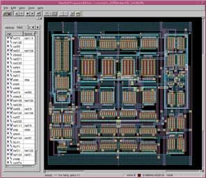
Tools like Neolinear's NeoCell automate the placement and routing of analog circuits. As with many digital designs, the engineers still do some routing manually, but automation shortens design time considerably.
Click on the image for the full illustration view.
Anthony Gadient, Neolinear's vice president of engineering, told IEEE Spectrum that NeoCell automatically places and routes analog cells at least three times as fast--and with equal or greater performance--than manual placement and routing [see figure].
But Verhoeven's op-amp group still relies on a layout editor to manually place and route circuits. He said he would not hesitate to use an automatic placement and routing tool if it performed as well as his designers did.
Sharing the synthesis spotlight
In addition to place and route capability, Neolinear also offers a circuit synthesis tool that automatically sizes analog transistors, a critical step in getting a working analog component. The size of an analog transistor determines how it will function with different input voltages. If the transistor is too small, even millivolts of fluctuations can push it out of the active region.
Besides Neolinear, three other companies--Barcelona Design, Analog Design Automation, and Antrim Design--have recently come out with tools billed as analog synthesis. But the companies all seem to have a slightly different interpretation of what, exactly, is meant by that term. None of the offerings resemble the digital approach of hardware-description-language in, netlist out. As long as people are not too picky about the meaning of synthesis, however, analog synthesis is definitely here and working, offering some method of turning high-level specifications for, say, operating voltage and speed into a working component.
Still skeptical of the whole lot is EDA analyst Gary Smith of Dataquest (now part of Gartner Inc., Stamford, Conn.). He has little confidence in these tools because the design methods to support them are not yet in place. Even so, Smith believes that they will be useful for retargeting existing chip designs to new manufacturing processes, which happens every 1218 months.
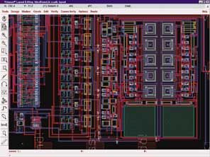
Software for editing a custom layout [above] is part of a larger analog/mixed-signal design package from Cadence Design Systems. While software can make the job easier, a layout engineer must still "push polygons" to manually place the circuits and draw the electrical connections between them.
Click on the image for the full illustration view.
Barcelona Design's tool, launched in February 2000, is available only through the Sunnyvale, Calif.based company's Web site. At the site, the designer is led through the selection of the manufacturing process and circuit topology to the addition of specifications and performance criteria. The tool then creates simulation set-up, netlist, schematic, and placement files that are intended for use with Cadence Design Systems' analog simulation and custom design tools [see figure].
Taking a different tack is Analog Design Automation Inc., in Ottawa, which is targeting analog companies with its analog synthesis technology based on fuzzy logic algorithms. Amit Gupta, president and CEO, said the company's technology offers a 2025-fold productivity increase over manual methods and results in higher-quality circuits. It is "Holy Grail technology," said Gupta, because it addresses the bottlenecks in analog design by enabling less-experienced engineers to produce high-quality analog designs.
Analog synthesis definitely can decrease the time between topology and schematic 10-fold, compared with the traditional manual method, agrees Felicia James, a mixed-signal product development manager at Texas Instruments in Dallas. It can also result in a better-quality circuit. Having all that tedious routine work automated, she said, lets the designers explore tradeoffs and fine-tune the circuit.
At Antrim Design Systems Inc., in Scotts Valley, Calif., the company's tool set captures specifications and topologies and generates detailed analysis, verification plans, and test suites. Antrim's strong point is its highly regarded mixed-signal simulator, which is coupled to the synthesis process. Matsushita Electric Industrial Co., Kodoma City, Japan, used Antrim tools to build single-chip DVD players and cell-phone components.
But along with its benefits, automation software for analog requires tradeoffs, not only in circuit performance, but also in the time needed to learn to use the software and fit it into the design flow. Designers will need to use the well-worn approach of considering which parts of the design need to be the "best of the best" and do those by hand. "The rest of the blocks only need to be very good," Carnegie Mellon's Rutenbar said, "and tools can do that. You don't need full custom for everything--you need to get it done in six months," not in two years.
From tools to methodologies
Tool vendors are pushing more than just tools. Everyone agrees that design methodologies must evolve as well. "Bottom-up analog design is a bottleneck to completing complex mixed-signal [system-on-chip] designs on schedule," said Michael Jackson, who heads the West Coast R&D group at Avant! Corp., Fremont, Calif. "The most promising area is the transition from bottom-up analog design to top-down design."
Texas Instruments' James said she's already seeing that shift occur. More information for the physical design of analog blocks comes from the chip-level description. "You used to have pure circuit designers," she said, "and the layout person was pretty separate from the design process." But now the AMS teams increasingly use the top-down methodologies, which means new job responsibilities for analog engineers.
For EDA to address the needs of AMS designers, EDA vendors must work closely with designers to understand the types of designs in progress, and to help create a coherent methodology that links the piecemeal tools, emphasized Henry Chang, an architect focusing on AMS issues at Cadence Design Systems. New tools will take a while to catch on, said Chang, and will be used only incrementally until designers trust and understand the limitations of the tool for their design types. There is no one-size-fits-all when it comes to EDA tools, so new design practices must fill the gaps.
More help on the way
Tools are still behind the curve in noise analysis and other problems--like harmonic distortion--that come with system-on-chip design. "Crosstalk and noise are critical in high-speed designs," said National Semiconductor's Verhoeven. Analog designers must consider noise, drift, temperature coefficients, jitter, nonlinear responses, and transmission line issues. Naturally, such disturbances affect the behavior of the analog circuits. Several companies specialize in developing tools for these aspects of analog design. For instance, Snaketech Inc., in Voiron, France, which was acquired last year by Simplex Solutions Inc., Sunnyvale, Calif., specializes in substrate noise.
Another up-and-coming technology that addresses the demands of analog circuitry is a field-programmable analog array (FPAA) from Anadigm Ltd., Crewe, United Kingdom. The technology is similar to the field-programmable gate array that is a staple of digital systems. The engineer uses software to select circuit elements from among 20 analog function blocks and connects them so as to perform the desired function. The selections are converted into a data stream and downloaded to the FPAA.
Functions that can be implemented using FPAA include offset removal, rectifiers, gain stages, comparators, and first-order filters. The designers can also construct high-order filters, oscillators, pulse-width modulators, and equalizers.
While this technology is very young, and still expensive, it could someday be useful for creating communications products that would work on any standard. For instance, a cell phone with a reprogrammable analog-to-digital converter would search the entire communications band for a signal, then grab the necessary program from memory to make itself into a code-division multiple access (CDMA), time-division multiple access (TDMA), or global system for mobile communications (GSM) phone. Such a phone could be used in Japan, Europe, or the United States without modification.
Testing, testing...
The requirements of testing mixed-signal designs open "a whole new frontier," according to David Yee, vice chair of the computer-aided design group of Semiconductor Research Corp., Durham, N.C., an organization that helps coordinate collaborative research among universities and industry. In fact, the cost per transistor of manufacturing test will soon exceed the cost of making the transistor--for some larger designs, it already has. In analog test, every transistor on the chip needs to be tested for behavior and performance, unlike digital testing, which only needs to check that the transistors switch. But currently, there are no good solutions to the AMS test problem.
For designs like phase-locked loops (PLLs), which keep certain input signals in sync with one another, current built-in self-test (BIST) structures will work fine. In other circuits, though, such measurements of performance as speed, dynamic range, and resolution cannot be made using BIST.
One issue is that there are sometimes no access pins to the analog block on a system-on-chip design. Yet some connection must link the analog block to the outside world. How to solve this problem is what drives Gordon Roberts, an associate professor in the department of electrical and computer engineering at McGill University in Montreal.
The way Roberts sees it, testing these tiny chips with huge machines just is not the best way. The trend has been to move the testers ever closer to the circuits on the chip. Even with centimeters between the circuits and the test equipment, degradation occurs in the measurement because of signal noise picked up by the electrical leads that connect the tester to the chip under test. To reach the embedded analog blocks, said Roberts, people are modifying the designs to bring signals from the circuits under test to the boundary of the chip. Some designers use drivers, buffers, and test buses on the chip to connect cores, embedded blocks of circuitry on system chips, to the outside world. But for Roberts, that's not enough.
"The way I see the world," said Roberts, "test instruments should have the same functionality as the benchtop equipment, but be located on the chip. Miniaturize the measurement instruments and add them as plug-in test cores."
For that kind of setup, the test cores would need to be small and scale to new process technologies. They should also be synthesizable from a hardware design language, which is where EDA can play a role. Once analog synthesis is mature, said Roberts, test-core blocks will be possible. Essentially, the test core would convert the analog signal to digital, and send that signal to a test pin on the boundary of the chip. With some improvements in the technology used to probe the pins while the chips are fresh from fabrication and still on the wafer, test could be made quite manageable.
Carnegie Mellon's Rutenbar agrees. With analog synthesis in place, designers will also be able to generate test vectors more easily. But right now, inserting BIST or other test structures is something analog designers avoid. "In analog, it's so hard just to get the signal path done," said Rutenbar, "they don't want to worry about putting test structures in."
Seeing eye to eye
The relationship between semiconductor makers and the EDA vendors is sometimes a thorny one. Some designers see the tools as immature, requiring them to create time-consuming work-arounds. Others, like National Semiconductor's Verhoeven, appreciate that EDA vendors allow users to add functionality to their programs with extra scripts. Fortunately, the pure analog chips are coming along just fine with the relatively mature simulation and layout editing tools.
Two things designers and EDA vendors do agree on is that there is always more room for automation and that tools need to be integrated into a more formal top-down design flow. But, said Cadence Design's Chang, "The analog productivity gap isn't a show-stopper. The industry adapts pretty well. People work it out."
Elizabeth A. Bretz & Linda Geppert, Editors
About the Author
BETH MARTIN is a free-lance science and technology writer in San Jose, Calif.
To Probe Further
For a peek into the analog community, browse the Planet Analog at https://www.planetanalog.com.


