Coaxing Light From Graphene
How a research institute near Barcelona exploits graphene’s potential in light-based technologies to advance 5G efforts


One day this past September, I found myself on a shuttle bus heading 20 minutes outside the center of Barcelona to the Institut de Ciencies Fotoniques, or ICFO (Institute of Photonic Sciences).
After five years of covering the groundbreaking photonics research coming out of this relatively small research institute nestled in the northeast corner of Spain, I figured it was time to visit the people and the facility that has had everyone buzzing since its participation at the 2016 GSMA Mobile World Congress. At this event, held in Barcelona that year, the world’s mobile network and device companies recognized that ICFO was offering a potential solution to a technological showstopper to the rollout of 5G networks: data centers that consume too much energy and don’t offer enough bandwidth.
At the Mobile World Congress, ICFO exhibited a prototype of a graphene-based integrated transceiver that could significantly reduce the power consumption of data centers, shrink their footprint, and increase their bandwidth. This has since led mobile companies such as Ericsson, Nokia, and Alcatel to lend support to ICFO’s research through their participation in the European Union’s US $1 billion research effort in all things graphene, known as the Graphene Flagship.

“We’re building an integrated transceiver fully packaged with 100-gigabyte-per-second data transfer,” said Frank Koppens, the leader of the quantum nano-optoelectronic group at ICFO, when we spoke at his offices at the ICFO’s modern facilities. “The plan is—together with the Graphene Flagship—to have a prototype in about two and a half years that will beat existing technologies.”
Koppens argues that these low-power, integrated photonic devices are required for the telecommunication industry’s transition to 5G, the next mobile telecommunications standard.
“This is a really big issue,” said Koppens. “5G cannot just scale. Some new technology is needed. And that's why we have several companies in the Graphene Flagship that are putting a lot of pressure on us to address this issue.”
There’s reason to believe that these graphene-enabled integrated photonic devices will be yet another groundbreaking development from an institution with a reputation for trail-blazing R&D.
The list of innovative graphene-related photonic research coming out of the ICFO is impressive: the first camera based on the integration of graphene, quantum dots, and CMOS technology, capable of imaging visible and infrared light at the same time; the use of graphene for creating “hot carrier” cells in photovoltaics; and the integration of a colloidal quantum-dot photodiode with a graphene phototransistor, paving the way for flexible 2D optoelectronics.
All of this research into graphene for photonics has fairly humble beginnings. Koppens recalls working on more or less traditional nanophotonics when he started to think about graphene’s potential for use in these applications.
Nanophotonic devices confine light to regions smaller than the optical wavelength and could ultimately prove useful for manipulating living cells or for ultrafast data processing. Despite years of progress, though, it has not been possible to fully modulate the optical response of nanophotonic devices. Graphene could help solve the modulation conundrum and make it possible for these devices to process and propagate data.

Excited by the idea that graphene could lead to a next generation of nanophotonics, Koppens recruited two other group leaders at ICFO: Gerasimos Konstantatos, who was working on a photodetector initially being targeted for photovoltaics, and Adrian Bachtold, who was working on nanomechanical resonators for sensors. Their collaboration has produced a steady stream of advances over the last few years.

“You start at the foundation of something like graphene and 2D materials and you soon realize that these graphene-related materials can actually be really disruptive in a number of areas,” said Koppens. “In my case, I completely changed my focus to 100 percent on graphene and other 2D materials.” This focus has led to the ICFO leading the photonics and optoelectronics work package for the EU’s Graphene Flagship.
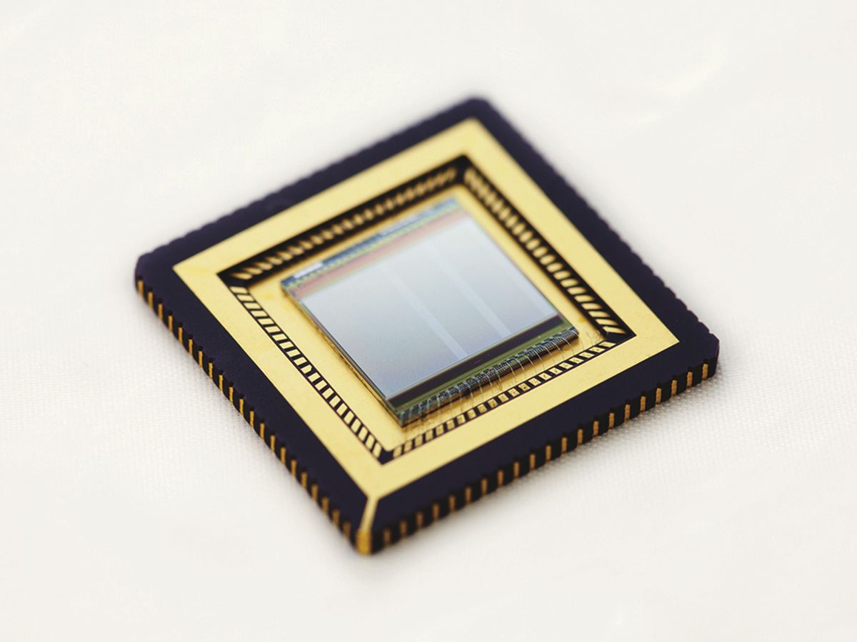
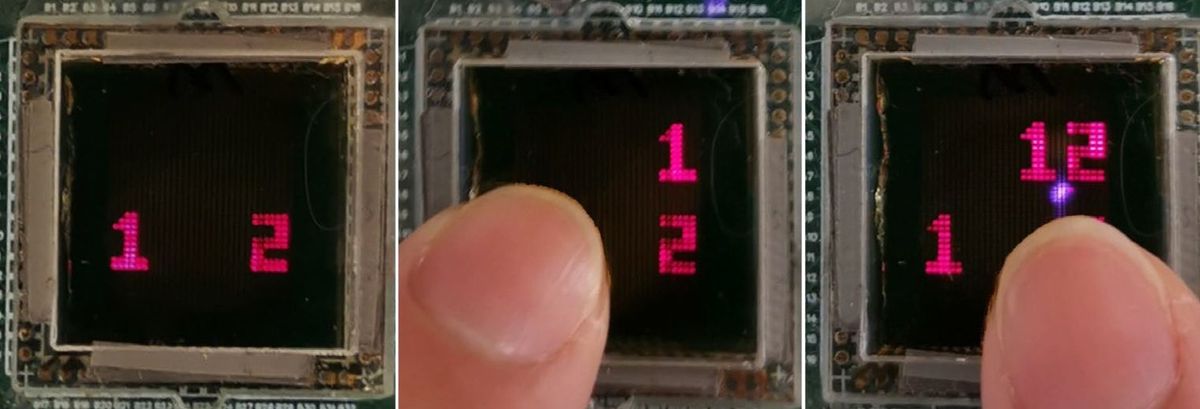
In September, the Graphene Flagship reported the fabrication of high-bandwidth graphene photodetectors for high-speed optical communications that were developed at another research institute but under the ICFO’s leadership. There is a direct link between these graphene photodetectors and ICFO’s development of a camera in which 120,000 photodetectors consisting of graphene and quantum dots are connected to CMOS circuitry.
In the video below, you can see a visualization of how these photodetectors—which are capable of detecting both visible and infrared light simultaneously—could make your smartphone a chemical detector or help you drive your car through fog.
ICFO has already developed a prototype camera based on the technology. However, not all the graphene-based CMOS circuits perform equally. Within five years, the aim is to improve the design of these graphene-based image sensors to operate at a higher resolution and in a broader wavelength range. Eventually, this camera could be designed to fit inside a smartphone or smart watch, according to Koppens.
While this camera is currently the only technology that allows for the detection of both visible and infrared light, its potential applications include enabling high-speed communications in optical networks.
In both multispectral imaging and ultrafast optical communications, one of the key issues has been the speed of the photodetectors. In 2015, ICFO researchers brought graphene photodetectors to the brink of terahertz speeds by getting their devices to convert absorbed light into an electrical voltage in less than 50 femtoseconds. To achieve these speeds, the ICFO team addressed the persistent issue of lengthy charge-carrier cooling times in graphene-based photothermoelectric devices, which has limited their switching speeds. By reducing those cooling times, ICFO has brought speeds down from picoseconds to femtoseconds.
These photodetectors perform on par with existing technology, but with the advantage that integration is much easier than with other semiconducting materials. ICFO is now working to combine the detector and modulator on one chip and on demonstrating an all-optical link.

For all these applications, synthesizing the best quality graphene has remained a challenge. While the quality of graphene needed to make these integrated devices has now become more available for larger areas through chemical vapor deposition (CVD), ICFO recruited Dmitri Efetov from Philip Kim’s lab at Harvard to lead its efforts in synthesizing and extracting the most from the full range of 2D materials.
“Besides graphene, there are thousands of other 2D materials,” said Efetov. “It’s probably safe to claim that maybe only five to 10 of those thousands have actually been studied. So I think the big goal is to really expand our knowledge of those thousands of other materials.”
In a recent paper published in Nature Nanotechnology, Efetov and his coauthors used one of the emerging materials in the flatlands universe known as two-dimensional transition-metal dichalcogenides (TMDs) to develop a light-emitting diode and photodetector for silicon photonic integrated circuits.
TMDs are made up of materials that combine one of 15 transition metals such as molybdenum or tungsten, with one of the three members of the chalcogen family such as sulfur, selenium, or tellurium. Researchers have investigated only a small number of the possible combinations of these TMD materials for electronic applications.
In this most recent research, Efetov and his colleagues produced a silicon waveguide-integrated light source and photodetector based on a p–n junction of bilayer molybdenum ditelluride. This TMD semiconductor has a direct bandgap, which is an energy band in which no electron states can exist and is essential for creating the “on/off” flow of electrons that are needed in digital logic electronics. The researchers believe that their fabrication technique should provide new opportunities for integrated optoelectronic systems that could enable the next generation of 5G telecommunications.
Koppens points out that technologies like these integrated photonic devices represent the same transition we witnessed in the integrated electronic circuits. “Integrated circuits really changed everything,” he adds, “and we believe with photonics this will also be the case.”


