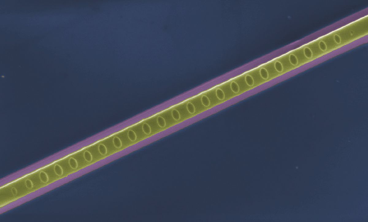
Scientists at the National Institute of Standards and Technology (NIST) have developed an underlying architecture for a new class of quantum photonic circuits—chip-based devices that leverage the quantum properties of light to process and communicate information.
In research described in the journal Nature Communications, the NIST researchers and their collaborators in China and the UK developed a class of devices that are composed of networks of low-loss waveguides and single-photon sources, all on a single chip. The resulting quantum circuit architecture could have an impact on photonic quantum computing and simulation, as well as metrology and communications.
Operating the device consists of producing streams of single photons, launching them into a network of waveguides and beamsplitters in which they are allowed to interfere with each other, and then detecting them at the network’s outputs.
To get a sense of the impact of this research, one must understand that until now, quantum information researchers have devised many types of systems to perform quantum simulations, metrology, and communications that rely on the interference of single, identical photons in large networks of waveguides and beamsplitters.
In these systems, photons are injected and will move around and interfere with each other randomly. Finally, they will come out at the output ports of the network, with a probability at each port that is determined by quantum mechanics. These probabilities are the final outcome of the experiment. Because of the inherent randomness of this process, the experiment has to be run a large number of times so that the probabilities can be determined with high confidence.
Unfortunately, there are three possible undesirable results. For one, the photons could get lost in the waveguides that compose the network. Another possibility is that the photons get lost in the process of launching them into the waveguides. And a final possibility is that if the photon source itself can only produce photons at a low rate, the experiment needs to run for much longer. For very large networks in particular, this could mean unrealistically long run times.
The NIST-developed architecture provides solutions to these three issues, allowing for them to be run much more efficiently, and enabling larger scale systems. To solve the photon loss in the waveguides, the NIST researchers used low-loss waveguides made out of silicon nitride. To address the issue of photons getting lost in their launch from the source to the waveguides, the NIST researchers have put the source directly on the chip, and created a geometry to launch them directly into the silicon nitride waveguides with high efficiency.
To overcome the third issue of low rate of photon production, the NIST team made a single-photon source based on a type of quantum dot that has been shown to produce indistinguishable single photons on-demand and at high rates (albeit at cryogenic temperatures).
“This is all done with mature, established integrated photonic fabrication techniques, that had been employed previously in non-quantum applications, and that are scalable—meaning that they can produce large circuits with large numbers of individual elements on them,” said Marcelo Davanço, a research scientist at NIST and first author of the paper.
The main difference between this device architecture and previous architectures, according to Davanço, is that the photon sources are on-chip, whereas in a great majority of other architectures, the photons are produced off-chip, then injected (many times with not great efficiency) into the on-chip waveguide network.
Davanço also contends that their architecture has advantages over other architectures that do include on-chip single-photon sources. “The main reason for that is that we use two types of materials with demonstrated high performance, and we found a way to combine them on a single chip in a way that their individual (and complementary) properties were not compromised and used almost to their full potential,” said Davanço.
A big reason for the superior performance of the quantum dots is that they are encapsulated deep inside a semiconductor material, gallium arsenide (GaAs), according to Davanço. GaAs is also advantageous because it has a high refractive index, and this is something that makes it possible to produce geometries that can efficiently capture photons produced by embedded quantum dots.
While GaAs may be great at boosting the quantum dots, it is not a good material for making low-loss waveguides. If a photon is produced by a quantum dot in the GaAs, and then launched into a GaAs waveguide, this photon will very soon either be scattered out of the waveguide, or absorbed by the material as it propagates.
“Our solution to this problem was to make a GaAs structure that could both efficiently capture photons emitted by an embedded quantum dot, and then another structure that could launch them with high efficiency into a waveguide made of a different material (silicon nitride), which was also known to provide considerably lower photon losses,” explained Davanço.
In continuing research, their aim is to fabricate devices with single quantum dots in them, rather than a large number, as in the paper. Davanço adds: “This will allow us to get a better idea of the level of indistinguishability that we can achieve within our architecture.”
Dexter Johnson is a contributing editor at IEEE Spectrum, with a focus on nanotechnology.


