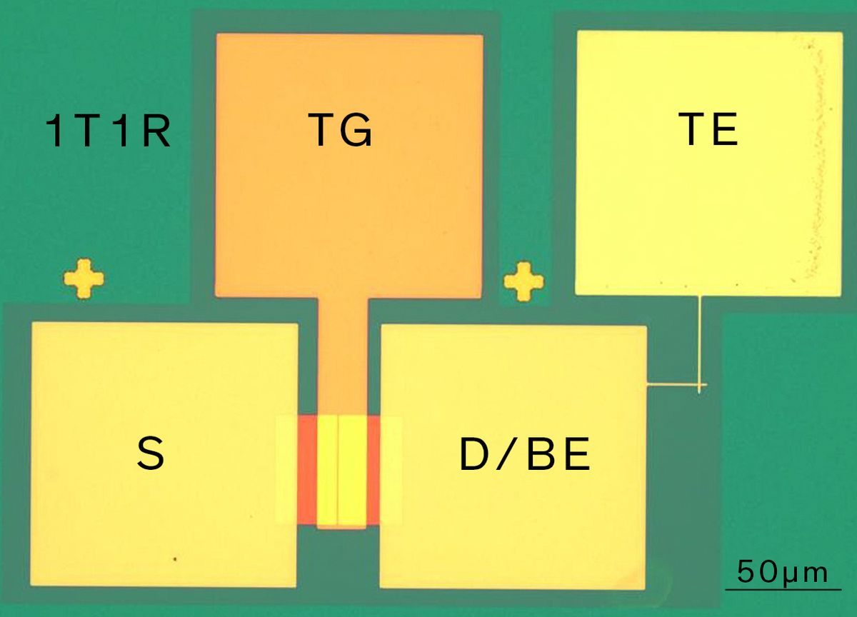
Researchers at Stanford University have demonstrated that field-effect transistors made from a single layer of molybdenum disulfide (MoS2) can successfully drive resistive random access memory. The results, which were reported last week at the IEEE International Electron Devices Meeting, represent a key milestone for the blending of memory with logic in a monolithic 3D integrated chip.
The chip the Stanford researchers developed is known as a 1-transistor-1-resistor memory cell. The architecture of these 1T1R memory cells offers enormous benefits over a memory array composed of memory cells with resistive random access memory (RRAM) and without a transistor.
Without the transistor, all the memory cells in a RRAM device end up being connected to various lines, rendering the memory array essentially a large resistor network. When one attempts to select one memory cell for reading, the read current will not only come from the selected memory cells in the memory array but also have currents in the form of leakage currents from all the unselected cells. Because of this leakage of current from the unselected cells, the voltage across the selected memory cell will be smaller than the applied voltage.
The benefit of having 1T1R memory cell is that the transistor can turn on and off and isolate the targeted memory cell from other memory cells, so that leakage current can be suppressed.
“While silicon-based FETs have been used for 1T1R memory cells, the advantage of monolayer MoS2 is that they can be transferred at low temperatures, making it possible to stack the memory layers and logic layers on top of each other in a monolithic 3D configuration,” said Rui Yang, a post-doctoral research fellow at Stanford and lead author of the research conducted within H. -S. Philip Wong’s Nanoelectronics Lab.
Yang added that the MoS2 field-effect transistor channel is atomically thin so that nanoscale interlayer vias, which serve as a kind of tunnel, can connect the different layers of the chip. This makes it possible to access memory from more parts of the chip with greater efficiency.
In general operation, RRAM operates as a memory device by storing data as resistance. For 1T1R-based RRAM, a memory cell is in writing mode when the field-effect transistor in the memory cells (in this case, a MoS2-based FET) is turned on. At this point, the transistors on the other unselected cells will be turned off, and the voltage will be applied on the top electrode of the selected RRAM and the source electrode of the MoS2 transistor.
This means that the transistor is connected in series with the RRAM. When the RRAM is changed from a high-resistance state to a low-resistance state, the top electrode of the RRAM is at high voltage, and the source electrode of the FET is grounded. The transistor drives the current through the RRAM and controls the compliance current, which in turn controls the resistance when the voltage periodically changes.
Currently, the fabrication of RRAM can be done with CMOS-compatible material. However, at the moment, industry is still not ready to manufacture 2D materials to the same degree, according to Yang.
“We need to find reliable ways to grow and transfer 2D materials in wafer scale, and integrate 2D transistors with RRAM in a monolithic 3D fashion,” he said.
In addition to growing and transferring 2D materials to the wafer scale, there are a number of issues that will need to be addressed with these devices. Yang believes they will need to achieve a smaller footprint, create a larger scale 1T1R array, and lower device variation. Nonetheless, he’s confident that technology holds a great deal of promise.
Both MoS2 and RRAM not only make it possible for lateral scaling, but also offer the possibility of vertical scaling through 3D stacking.
Yang added: “Toward that, we have plans to fabricate multiple memory and logic layers for a 3D circuit, with the capability of in-memory computing.”
Dexter Johnson is a contributing editor at IEEE Spectrum, with a focus on nanotechnology.


