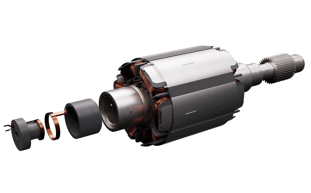
A digital schematic of Mapper Lithography's maskless electron beam lithography device
When it comes to making denser, smaller circuits, all eyes have been on extreme ultraviolet lithography (EUV). But it turns out that an alternative technology that uses electron beams to draw features might be just as productive and even cheaper.
“I think Moore’s law has pushed MEMS and electronics to the point where we can afford it,” says Burn Lin, who spearheads nanolithography at the foundry giant Taiwan Semiconductor Manufacturing Company, Ltd.
Lin, who stopped briefly by the IEEE International Solid-State Circuits Conference in San Francisco, says TSMC has been testing the capabilities of a “pre-alpha” tool made by MAPPER that uses 110 electron beams to write chip features. The company has also been kicking the tires on a machine called the REBL made by KLA-Tencor.
Years ago, e-beam lithography was dismissed by some industry watchers as too slow to be a good and inexpensive way to make wafers (the speed was once considered so unimpressive that the technology made IEEE Spectrum’s losers list in 2004).
But Lin says TSMC now suspects the tools could be used to pump out as many as 150 wafers per hour, about the same rate that today's lithography tools can muster. What’s more, he’s calculated that the cost of wafers made with e-beam lithography will be roughly one-third less than that of wafers made with EUV. Once the industry shifts from LP-record-sized 300-millimeter wafers to 450-mm wafers, the technology is likely to be even more affordable—just 57 percent of the cost of making wafers using EUV lithography. “It’s the only way I know to reduce costs while shifting to a larger wafer size,” says Lin, who prepared the numbers for a talk last week at the SPIE Advanced Lithography conference in San Jose, Calif.
TSMC hasn’t abandoned EUV, but Lin notes that the window for introducing the technology is shrinking. Once eyed for 60-nanometer chips, EUV may possibly be ready in a few years, just in time to produce 14-nm chips. But unlike e-beam lithography, the technology might not be useful past the 10-nm level, Lin says. To boost the resolution, the aperture of EUV optics has to increase, too. Just as in a camera, that larger opening shortens the depth of focus. The EUV light could therefore be rendered spottily effective as it encounters slight variations in height along the wafer's surface.
What’s changed for electron beam lithography? Lin says advances in chip performance and the micromachining technology needed to manipulate the electron beams have been key factors. If e-beam lithography manages to catch on, lithography will become part of the cycle of Moore’s law in a way that it hasn’t before—better chips will mean better lithography tools. As Lin puts it: “it’s using Moore’s law to improve Moore’s law.” And what could be more elegant than that?
Image courtesy of Mapper Lithography
Rachel Courtland, an unabashed astronomy aficionado, is a former senior associate editor at Spectrum. She now works in the editorial department at Nature. At Spectrum, she wrote about a variety of engineering efforts, including the quest for energy-producing fusion at the National Ignition Facility and the hunt for dark matter using an ultraquiet radio receiver. In 2014, she received a Neal Award for her feature on shrinking transistors and how the semiconductor industry talks about the challenge.