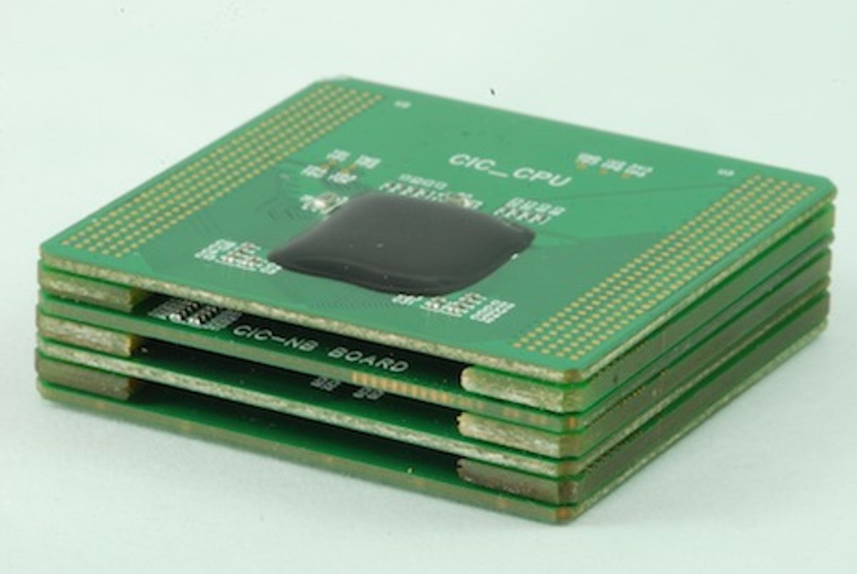
A Taiwanese R&D center says it has come up with a packaging technology that will speed development of multi-chip systems.
Taiwan's National Chip Implementation Center (CIC) calls the technology MorPACK, for morphing package. MorPACK is three-dimensional (3D) embedded system integration platform that can integrate several different kinds of chips. CIC says the technology will cut down development time and cost, because it allows for the easy integration of chips with different functions into one tightly-bound package.
MorPack is a stack of sub-modules, which are each composed of bare chips, a fiberglass and copper substrate, connection bridges, and solder balls.
The lower part of the structure, called the common platform, consists of a processor, a north-bridge (a chip linking the processor to memory chips), synchronous DRAM, NOR flash memory, and a south-bridge (a chip linking the processor to peripheral devices). The upper part, called the custom substrate , is designated for a chip the user wishes to develop as the unique part of the system. This can be an IC designed to accelerate some specific function, such as decryption, or a programmable logic chip (FPGA).
"The MorPACK platform was invented to share part of electronics developers' workload,” says Chun-ming Huang, who leads the MorPACK development team at CIC. “They now just need to spend time and money tapping out accelerator [intellectual property] cores invented by themselves rather than on the whole module."
The CIC spent two years designing the MorPACK platform. The hope was to provide more integration to university designers than was allowed by university-serving prototyping systems, such as Multi-Project System-on-a-chip (MP-SoC). Although the MP-SoC concept has greatly reduced fabrication cost of SoC designs, you can’t integrate fundamentally different types of chips onto the same piece of silicon.
Huang stressed that the MorPACK technology allows electronics developers to stack chip modules with different functions on top of each other. Therefore, it can help save space and resources on a carrier board. "The dense three-dimensional structure guarantees better performance and less power demand than that of a huge two-dimensional complex IC board,” Huang says.
Right now, the MorPACK platform is 4 x 4 centimeters, but Huang says that his team has evaluated the possibility to shrink it. "We aim to downsize it to one fourth next year, by adopting the (more expensive) flip-chip packaging technology, without compromising existing advantages," he says.
In Taiwan, seven research teams at six universities have adopted the MorPACK platform to develop IP cores needed by intelligent systems for biomedical, 3D communication, image processing and other applications. According to Tzi-dar Chiueh, the director general of CIC, for each IP core-design project, the reusable MorPACK platform on average helps researchers cut down development time by three to six months and reduce cost by NT$ 1.5 million ($50,850).
Chiueh says the center plans to transfer the technology to the private sector next year.


