
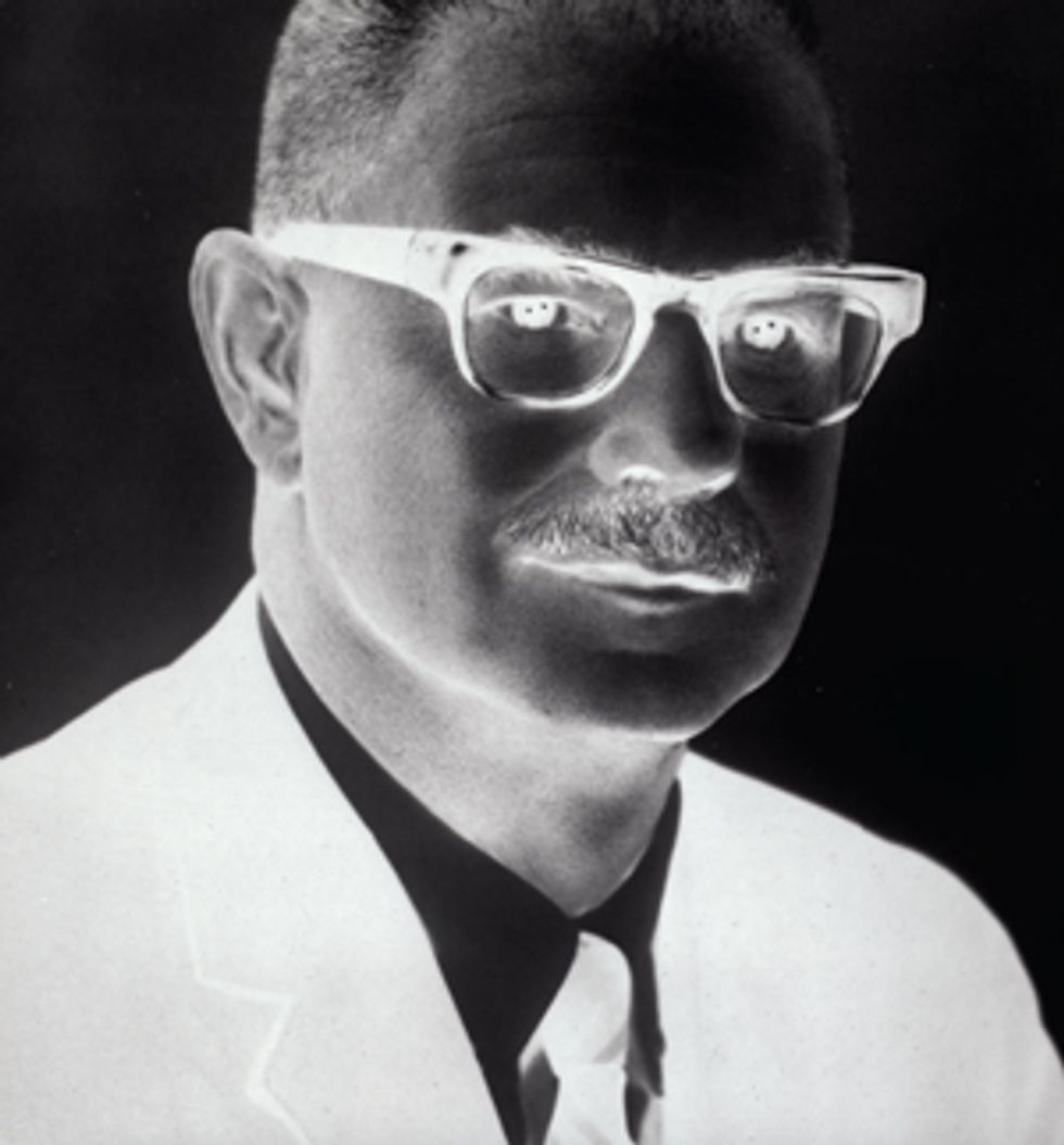
 Flawed Hero: Jack A. Morton led Bell Labs’ effort to transform the transistor from a research curiosity into a commercial product. But his aversion to microchips would later cost AT&T dearly.Photo: AT&T Archives and History Center
At 4:15 a.m. on 11 December 1971, firemen extinguishing an automobile blaze in the New Jersey hamlet of Neshanic Station were shocked to discover a badly charred body slumped face-down in the back seat. It proved to be the remains of Jack A. Morton, the vice president of electronic technology at Bell Telephone Laboratories, in Murray Hill, N.J. He had last been seen talking with two men at the nearby Neshanic Inn just before its 2 a.m. closing—about 100 meters from the abandoned railroad tracks where his flaming Volvo sports coupe was spotted. Local police quickly arrested and booked the men for murder.
This gruesome slaying ended the stellar career of the man who had led Bell Labs’ effort to transform the transistor from a promising but rickety laboratory gizmo into the sturdy, reliable commercial product that eventually revolutionized electronics. During the 1950s and 1960s, Bell Labs’ golden age, Morton served as quarterback of the device development team, making nearly all the key calls on which technologies to pursue and which to forgo. He was a bold, forceful, decisive manager who didn’t suffer fools gladly. And with some of the world’s most intelligent and innovative researchers working for him, he rarely had to.
Morton didn’t always make the right decisions, however. As one of his former colleagues observed, decisive leadership can easily become a flaw rather than a virtue [see photos, "Flawed Hero”]. On integrated circuits in particular, Morton exhibited serious blind spots that cost the parent phone company, AT&T, dearly—and may have contributed to its eventual dismemberment. But his untimely death meant that he would not be around to witness the consequences of his choices.
Like so many of the leading figures in the semiconductor industry—John Bardeen, Nick Holonyak, Jack Kilby, Robert Noyce—Jack Morton was born and raised in America’s pragmatic heartland. After growing up in St. Louis, he matriculated at Wayne University, in Detroit, where he was a straight-A electrical engineering major as well as quarterback of the football team. He was avidly pursuing graduate work in the discipline at the University of Michigan, intent on an academic career, when Bell Labs research director Mervin Kelly happened to visit in 1936. Kelly offered the promising young engineer an R&D position. Morton accepted, planning to pursue a Ph.D. in physics at Columbia University simultaneously. At Bell Labs, he started the same year as John Pierce, who would go on to pioneer satellite communications; Claude Shannon, who would lay the foundations for information theory; and William Shockley, who would share the Nobel Prize for inventing the transistor.
A visionary firebrand, Kelly had directed vacuum-tube R&D at the Labs [see photos, "Early Promise”]. He was keenly aware of the limitations of the bulky, power-hungry devices and the problems with the electromechanical relays then used as switches to connect phone calls throughout the Bell System. He envisioned a future when this switching would be done completely by electronic means based on the solid-state devices that were beginning to find applications in the late 1930s. To realize his dream, he hired the best scientists and engineers he could cajole into working in an industrial laboratory.
World War II put the project on hold. Kelly played a major wartime role, heading up radar development at Bell Labs and the Western Electric Co., AT&T’s manufacturing arm. Morton, too, did important military work. Having plunged into the intricacies of microwave circuit engineering just before the war, he helped design a microwave amplifier circuit that extended the range of radar systems and gave Allied forces in the Pacific a key advantage.
After the war, Morton developed a peanut-size vacuum triode that could amplify microwave signals. This triode served at the heart of the transcontinental microwave relay system that AT&T began building during the late 1940s, and it continued to be used in this capacity for decades, permitting coast-to-coast transmission of television signals.
By 1948, Morton had achieved a reputation as an imaginative engineer who knew how to get sophisticated devices into production. One day in June, Kelly tersely summoned him to his office. Such a one-on-one encounter was not to be taken lightly, for Kelly—who had risen to executive vice president—had a legendary temper. A friend of Morton’s later described the meeting as follows:
“Morton,” Kelly began, “You do know about the work we’ve been doing on the transistor?”
“Yes, sir,” Morton replied a bit hesitantly. He’d heard through the grapevine about the transistor, the secret new solid-state amplifier invented the previous December by Bardeen and experimental physicist Walter Brattain, but he was unsure whether to admit it. “At least I know it’s pretty important.”
“Morton, I’m going to be away for the next four weeks,” Kelly proceeded imperiously. “When I get back, I would like to see a report from you on the transistor. I want you to tell me how to develop it commercially.”
Kelly didn’t know it, but Morton had been running scared of him ever since being hired, and he was now terrified at the prospect of failing on such an enormous assignment. For the next three weeks Morton talked to the scientists and engineers working on transistors but made little progress. Then, in the last week, he somehow pulled it all together and had a 46-page report waiting on the boss’s desk when he returned. Kelly read it, approved it, and immediately put Morton in charge of transistor development.
Bardeen and Brattain’s point-contact transistor was a crude, fragile device consisting of two closely spaced metal points jabbed into a germanium sliver. That it worked at all was a minor miracle. Already a pilot production line at the Labs was turning out hundreds of prototypes every week for further experimentation, measurement, and testing. But the transistors were extremely noisy, variable, and unreliable. “In the very early days, the performance of a transistor was apt to change if someone slammed a door,” Morton was quoted as saying in a 1953 article in Fortune.
In the fall of 1948, he gathered about a dozen engineers and a similar number of technicians for a meeting to launch his transistor development team [see photos, "Team Leader”]. According to two of his lieutenants, Eugene Anderson and Robert Ryder, Morton already seemed to anticipate that their work would make history: “We shall change the world,” he prophesied. “In what manner I do not know, but change it we will.”
The team attacked the noise and reliability problems on several fronts, and by mid-1949 they had two improved versions ready for production, one to amplify signals and the other for switching applications. Western Electric began manufacturing the transistors in 1950, and Bell System engineers soon found uses for them. The first commercial application was in a tone generator used in toll-call signaling.
Morton also had the foresight to pursue what became known as “fundamental development” of basic manufacturing processes and technologies that could have across-the-board implications for the new semiconductor industry. A prime example: when the chemist Gordon Teal could not convince his own department head to let him grow large single crystals of germanium for use in making transistors, he appealed to Morton for support. Coming from electron tube manufacturing, Morton understood that transistor action demanded a near-perfect medium—like the vacuum in a tube—and so he readily came up with the pittance required to buy or build the necessary crystal-growing equipment. Dollar for dollar, it was probably the best investment in Bell Labs’ history.
Morton knew how to get research ideas and designs out of the Labs and into manufacturing at Western Electric, too. Here the groundwork had been laid by his mentor, Kelly, who during the war had recognized the obstacles to transferring technology from an isolated central lab. He felt it was crucial to have people familiar with the latest scientific and technological advances working right on the shop floor, especially when fabricating high-tech components. And so, after 1945 he established a system of branch labs at several Western Electric plants, consisting of teams of Bell Labs employees focused on production engineering and acting as liaison with their colleagues back in Murray Hill.
Morton fine-tuned this approach at the new Western Electric plant in Allentown, Pa., which produced electronic devices and components for the Bell System. He set up a semiconductor development group there and put Anderson in charge. A tube engineer who had been with Morton’s Murray Hill transistor team from the outset, Anderson had a good grasp of the necessary solid-state physics and semiconductor technology.
So Morton’s development team was poised to move quickly in mid-1951 when Bell Labs announced the successful fabrication of the junction transistor, much more rugged and practical than the delicate point-contact device invented by Bardeen and Brattain. Conceived by Shockley and fashioned by chemist Morgan Sparks using Teal’s crystal-growing apparatus, this three-layer germanium sandwich had a much simpler structure than the point-contact transistor and far outperformed it. That the junction transistor would be the preferred path to commercialization was immediately obvious. And Morton’s group led the way, getting the device into production within a year.
In the beginning, transistors were made of germanium, not silicon. Although germanium’s lower melting point makes it far easier to purify, transistors crafted from it are sensitive to temperature changes. And they make lousy switches: tiny leakage currents continue to flow even when the devices are nominally off. Silicon doesn’t have these problems, but it’s a lot more difficult to work with. In the early 1950s, only a few farsighted researchers like Shockley recognized that silicon was the semiconductor material of the future.
In 1954 Morris Tanenbaum fabricated the first silicon transistor at Bell Labs [see “The Lost History of the Transistor,” IEEE Spectrum, May 2004]. Later that year AT&T executives decided to pursue the first electronic switching system—known as ESSâ''1—based on semiconductor devices rather than electromechanical crossbar switches. A trial run was set to begin in 1958.
Morton faced a crucial decision: whether to employ the (by then) well-established germanium technology or bet the house on silicon, which still had a long way to go in development and was thus far riskier. Both Sparks and Tanenbaum, who worked on the research side of the fence and didn’t have to worry about manufacturing devices of extreme reliability, now say in hindsight that the choice to go with silicon was obvious. At the time, however, it was anything but.
In March 1955 Tanenbaum improved on his earlier invention by diffusing impurities into the silicon. This process allowed him to fashion a narrow base layer—the “meat” in the semiconductor sandwich—only about a micrometer thick. The device, which came to be known as a diffused-base transistor, could amplify and switch signals above 100 megahertz, into the range of FM radio and television. Best of all, such a high switching speed, about 10 times that of previous silicon transistors, meant that it could be used for electronic switching.
When he heard the news, Morton was in Europe. He immediately canceled his travel plans and rushed back to Allentown. “On a snowy, miserable day,” recalled Anderson, Morton decreed that ”it was to be in silicon as a material and diffusion as a technology that future transistor and diode development would move in the Bell System.”
His bold decision proved correct. Bell Labs researchers soon resolved the difficulties with purifying silicon and growing crystals of it. They then discovered how to make a glassy, protective oxide layer on the silicon surface that could be used to pattern the impurity diffusions. Fairchild Semiconductor Corp., in Mountain View, Calif., led by Robert Noyce, would adapt these silicon technologies to produce the first commercial microchips in 1961. Western Electric, in turn, used Fairchild’s patented planar process to make diffused-base silicon transistors for the Bell System’s ESS-1, which began to show up in phone exchanges in the early 1960s [see photo, "From Lab to Factory”]. Kelly’s dream of electronic switching finally became reality, thanks in part to Morton’s courage and vision.
It is a remarkable historical fact that Bell Labs did not invent the microchip, despite having developed almost all the underlying technology that went into it. This puzzling failure can be attributed partly to market forces—or the lack of them. As former Bell Labs President Ian Ross once explained in an interview, the Labs focused on developing robust, discrete devices that would enjoy 40-year lifetimes in the Bell System, not integrated circuits. Indeed, the main customers for microchips were military procurement officers, who, especially after Sputnik, were willing to cough up more than US $100 a chip for this ultralightweight circuitry. But the telephone company had little need for such exotica. “The weight of the central switching stations was not a big concern at AT&T,” quipped Ross, who back in 1956 had himself fashioned a precursor of the microchip.
Ultimately, though, the company would need integrated circuits. Think of the Bell System as the world’s largest computer, with both analog and digital functions. Its central offices put truly prodigious demands on memory and processing power, both of which could be best supplied by microchips. And it was microchips driven by software that eventually made electronic switching a real success in the 1970s. But by then AT&T was playing an increasingly desperate catch-up game in this crucial technology.
Here Morton was partly to blame. He pooh-poohed the potential of microchips and large-scale integration. Citing his own version of the “tyranny of numbers,” he initially argued that the manufacturing yields on integrated circuits would become unacceptably low as the number of components on a chip grew. Even though each chip component—typically a transistor—might be made with a 99 percent success rate, this number would have to be multiplied by itself many times, resulting in abominable yields, he reasoned. Tanenbaum summed up Morton’s attitude this way: “The more eggs you put in the chip basket, the more likely it is that you have a bad one.”
And reliability would suffer, too, or so Morton thought. Due to his lofty position—he had become a vice president in 1958—this argument dominated the thinking at Bell Labs in the early 1960s. “Morton was such a strong, intimidating leader,” observes Eugene Gordon, who worked for him then, “that he could make incorrect decisions and remain unchallenged because of his aggressive style.” Morton’s previous string of successes probably contributed to his sense of his own infallibility.
But his tyranny hypothesis ultimately didn’t hold up. Failure rates of microchip components are an average over the entire surface of a silicon wafer. Each wafer can have unusually bad regions that pull the average down significantly, while chips in the better regions have much higher success rates, leading overall to acceptable yields. It took outsiders from the Sun Belt—at Fairchild and Texas Instruments—to overthrow the tyranny and pioneer microchip manufacturing.
Well into the 1960s, Morton continued to drag his feet on silicon-based chip technology, despite mounting evidence of its promise. He did not consider it a sufficiently “adaptive” technology, by which he meant something that could easily respond to the evolving needs of the Bell System and gradually incorporate innovative new materials and techniques as they became available. The phone company couldn’t use a technology that was too disruptive, because the systems engineers at AT&T always had to ensure extreme reliability, compatibility with existing subsystems, and continuity of telephone service. “Innovation in such a system,” Morton declared, “is like getting a heart transplant while running a 4-minute mile!”
To the dismay of Gordon and others in his division, Morton squelched efforts at Bell Labs to pursue what the semiconductor industry began calling large-scale integration, or LSI, which yielded single silicon chips containing more than 1000 components. He even derided people working on LSI as “large-scale idiots,” said one colleague. Instead, he promoted the idea of hybrid technology incorporating smaller-scale microchips, which could be manufactured with higher yields, into “thin-film” circuits based on metals such as tantalum, in which resistors and capacitors could be etched more precisely than was possible in silicon. Morton championed this approach as the “right scale of integration,” or RSI—another favorite phrase of his.
It proved to be a bad decision, but Morton was adamant. Tanenbaum reckons that it cost AT&T two or three years’ delay in getting microchips into the Bell System for later versions of electronic switching. Even then, the phone company had to purchase most of those chips from other companies instead of making them at Western Electric. Buying components from outsiders was something AT&T had tried to avoid before 1968 (when forced to by a landmark decision by the Federal Communications Commission), because that made it more difficult to control their operating characteristics and reliability.
Bell Labs’ focus on robust discrete devices, almost to the exclusion of microchips, started to dissolve in the late 1960s. Engineers at Murray Hill and Allentown began working again on the metal-oxide semiconductor (or MOS) field-effect transistor, which Bell Labs had pioneered in the 1950s and then ignored for half a decade—even as companies like RCA, Fairchild, and others ran with it. In a MOS field-effect transistor, current flows through a narrow channel just under the oxide surface layer, modulated by the voltage on a metal strip above it. As the number of components per microchip swelled, the simple geometry and operation of the MOS transistor made it a better option than the junction transistor.
But Fairchild engineers had already solved most of the challenging reliability problems of MOS technology in the mid-1960s, so that company enjoyed a big technological advantage as the devices began finding their way into semiconductor memories.
Once again, it had been Morton’s decision back in 1961 not to pursue the development of MOS devices, in part because they initially exhibited poor reliability and didn’t work at high frequencies. As Anderson recalled, “Morton, who was ever alert to spot a technology loser as well as a winner, was thoroughly convinced of the inherent unreliability of surface devices, as well as…that field-effect devices would be limited to low frequencies.” In the early 1960s, they indeed made little sense for a company already heavily committed to electronic switching based on discrete devices. But when Bell Labs and AT&T began embracing MOS transistors later that decade, they were once again playing catch-up [see “The End of AT&T,” Spectrum, July 2005].
His dim view of microchips didn’t prevent Morton from being showered with accolades from the mid-1960s onward. In 1965, he received the prestigious David Sarnoff Medal of the IEEE for “outstanding leadership and contributions to the development and understanding of solid-state electron devices.” Two years later, he was among the first people to be inducted into the U.S. National Academy of Engineering. In 1971, Morton published an insightful book, Organizing for Innovation, which espoused his “ecological,” systems approach to managing a high-tech R&D enterprise like Bell Labs. In it, he expounded at length on his ideas about adaptive technology and the right scale of integration. Morton was also in demand as a keynote speaker at industry meetings and as a consultant—especially to emerging Japanese electronics and semiconductor companies, where his word was revered.
But there was a dark side to Morton’s personality that few of his Bell Labs colleagues ever glimpsed at work. He had a serious drinking problem, probably exacerbated by his frustration at his stagnation within the Bell Labs hierarchy. Sharing drinks with Gordon one evening, Morton confided his disappointment that he was still only a vice president after more than a dozen years at that level. Ambitious and aggressive, he yearned for the role of chief executive. Morton also had difficulties at home, and he began spending more evenings at the Neshanic Inn, a local hangout about a mile from where he lived.
Sparks vividly remembers how he was playing golf with Bell Labs president James Fisk that balmy Saturday morning in December 1971 when an anxious messenger rushed out onto the course to give them the tragic news of Morton’s death. Ashen-faced, Fisk asked Sparks to check into what had happened. Sparks went to the hospital where the autopsy was being performed. The doctor told Sparks that Morton’s lungs were singed, indicating he was still alive and breathing when the fire was ignited.
Details of what happened that fateful night came out at the murder trials of the two men, Henry Molka and Freddie Cisson, which occurred the following fall at the Somerset County Courthouse, in Somerville, N.J. According to prosecutor Leonard Arnold, Morton had just returned from a business trip to Europe and was driving back from the airport when he decided to stop by the inn for a drink. But it was nearly closing time, and the bartender refused to serve him. Molka and Cisson told Morton they had a bottle in their car and offered to pour him a drink. They walked out with him to the parking lot and mugged him there, pocketing all of $30.
Gordon figures they thought Morton an easy mark, a well-dressed man in his late 50s with a showy gold watch. But they were mistaken. Morton kept himself in good physical condition and, given his aggressive disposition, probably fought back. A violent struggle must have ensued. After knocking him unconscious, Molka and Cisson threw him in the back seat of his Volvo, drove it a block down the road, and set it on fire with gasoline they extracted from its fuel-injection system. The two men were convicted of first-degree murder and sentenced to life imprisonment, but according to Arnold, they served only 18 years.
Sadly, the world had lost one of the leading proponents of semiconductor technology, the articulate, visionary engineer who turned promising science into the extremely useful, reliable products that were already revolutionizing modern life by the time of his death. Under Morton’s leadership as head of electronics technology at Bell Labs, many other innovative devices were invented that today are ubiquitous in everyday life, including flash memory and the charge-coupled device, both derived from MOS technology. But like the microchip and the MOS transistor, they would be developed and marketed by other companies.
“Jack just loved new ideas,” said Willard Boyle, one of the CCD’s inventors. “That’s what fascinated him, where he got his kicks.” That attitude is probably an important part of the reason that Bell Labs served as such a fount of innovative technologies under his stewardship. But AT&T could realistically pursue only a fraction of these intriguing possibilities, so the Labs focused mainly on the discrete devices and circuits that Morton and other managers considered useful in implementing their immediate, pressing goal of electronic switching. Viewed in that context, the decision to pass on yet another revolutionary, but unproven, technology made good business sense—at least in the short run.
Thus, another, more subtle tyranny of numbers was at work here. Given the seemingly infinite paths that AT&T could follow—and the legal constraints on what it could actually make and sell—it was probably inevitable that outsiders would eventually bring these disruptive new technologies to the masses.
About the Author
Contributing Editor MICHAEL RIORDAN is coauthor of Crystal Fire: The Birth of the Information Age. He teaches the history of physics and technology at Stanford University and the University of California, Santa Cruz.
To Probe Further
An obituary of Jack Morton, written by Morgan Sparks for the National Academy of Engineering, is available on the Web at https://darwin.nap.edu/books/0309028892/html/223.html.
Chapters 9 and 10 of Michael Riordan and Lillian Hoddeson’s Crystal Fire (W.W. Norton, 1997) discuss the invention and development of the junction transistor at Bell Labs. A tutorial on the device, ”Transistors 101: The Junction Transistor,” appeared in the May 2004 issue of IEEE Spectrum.
Jack Morton’s Organizing for Innovation: A Systems Approach to Technical Management (McGraw-Hill, 1971) fleshes out his management philosophy.
Chapter 1 of Ross Knox Bassett’s To the Digital Age: Research Labs, Start-up Companies, and the Rise of MOS Technology (Johns Hopkins University Press, 2002) contains the definitive history of the MOS transistor.