
Five years ago, Intel introduced today’s high-performance transistor to the world. Dubbed the FinFET, the device takes its name from its appearance: The transistor’s current-carrying channel sticks up vertically in the shape of a fin, and the gate that controls it drapes over the sides. The result is a much tighter control over the flow of current, which in modern microprocessors can fairly easily sneak across the transistor when it’s supposed to be shut off.
But well before the FinFET exploded onto the scene in 2011, engineers and device physicists had already been looking at the possibility of taking that transistor geometry to its logical conclusion, with a gate that completely surrounds the current-carrying channel. Shifting to such a “gate-all-around” geometry would, in theory, allow chip companies to produce shorter transistors that don’t leak copious amounts of current, improving speed or power consumption in the process.
Now, Hans Mertens and colleagues from the nanoelectronics research firm Imec, based in Leuven, Belgium, have constructed gate-all-around transistors from dense stacks of 8-nanometer-wide nanowires on a conventional silicon surface. Although engineering hurdles remain, the coming years could see further improvements to this basic approach—and perhaps its introduction into mass manufacturing.
Gate-all-around devices can be made by orienting a nanowire made of semiconducting material in one of two ways: laterally, as today’s transistor channels are arranged, or vertically, so that the nanowire stands on end, perpendicular to the plane of the chip.
The Imec team, which presented its findings at theSymposia on VLSI Technology and Circuits, held in June in Honolulu, took the lateral approach. They began by growing alternating layers of silicon and a silicon germanium mix. The team then etched away parallel trenches, leaving behind fins containing these alternating layers—a bit like pillars of rock with different sedimentary strata. In a later step, the team etched away the remaining silicon germanium, leaving behind two silicon nanowires in each erstwhile fin.
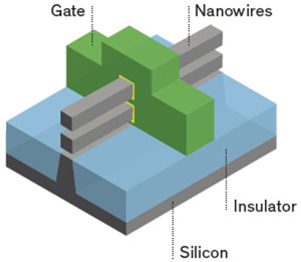 Fin Evolution: Transistors made with stacks of horizontal nanowires take a page from the finlike devices used today. The gate material wraps around each channel to provide better control. Stacking the nanowires boosts current density.Illustration: Erik Vrielink
To create a transistor, insulating material and then metal gates were added around each nanowire to form the gate structure. And for each vertical pair of nanowires, the source and drain regions—the places where current originates and winds up—were connected so they would become part of the same transistor. Stacking the nanowires boosts the amount of current that can pass through a given area of transistor—and thus how much can pass through a given area on a chip.
The great advantage of this approach, explains Imec logic program managerNaoto Horiguchi, is that the fabrication process is quite close to that used to make the FinFET transistors in today’s high-performance chips. “This is kind of a natural extension from FinFET to the next generation,” he says.
Imec’s is the first demonstration of stacked-nanowire devices at such a small scale, saysMichael Guillorn of IBM’s Thomas J. Watson Research Center in Yorktown Heights, N.Y. Guillorn has been involved with IBM’s gate-all-around device research program since 2009.
IBM presented results at last year’s VLSI event that explored the limits of performance for a single layer of horizontal nanowires at an advanced chip manufacturing level. Because resistance increases as a channel narrows, a common concern has been that nanowires would too strongly resist the flow of current, Guillorn says. But the IBM group’s results suggest that is not the case. They also suggest that more ribbonlike nanowire structures—wide and flat instead of square or round in cross section—could help improve performance.
There is still plenty of work to be done. One focus at Imec, Mertens says, is on ways to better isolate the gate that surrounds the channel of the nanowire from the source and drain regions. Because the source and drain are so close to the gate in the small device, they tend to exchange energy via capacitive coupling.
Guillorn says researchers are, one by one, “knocking things off the list of reasons” why nanowires might not be desirable. Assuming engineers work out all the kinks in manufacturing and performance, the devices could potentially enter chipmakers’ production lines in three to six years, he says. The timing will hinge on how long companies believe they can extend the FinFET, the cadence at which they decide to introduce future generations of chips, and how aggressive they want to be with the underlying technology. “Early adoption of gate-all-around,” Guillorn says, “is a great way for a semiconductor company to differentiate itself.”
This article appears in the October 2016 print issue as “The Next High-Performance Transistor.”