
This is part of IEEE Spectrum’s special report: Winners & Losers VII
In March 2006, Sony dashed the hopes of gaming fans by postponing the supposedly imminent launch of its PlayStation 3 console until November. Six months later, it pushed back the launch again. Later it revealed it couldn’t live up even to that promise: Although the launch went ahead in Japan and the United States, European shops got the console only in the first quarter of 2008, and Sony’s shipments in the first few months were only half as big as it had intended.
What went wrong? Sony would say only that it had had trouble manufacturing a new type of semiconductor laser that emits violet light, which has waves short enough to read the densely packed data of a Blu-ray disc. However, informed observers—including Shuji Nakamura, who invented this class of laser—had no doubt that the specific problem was a lack of decent gallium nitride substrates on which to grow the laser chips.

A lot of big materials suppliers are in the race, but a dark horse called NanoGaN seems likely to win it. The company, a spin-out from the electrical engineering department of the University of Bath, in England, can make gallium nitride substrates of high quality—and what’s more, it can recycle them, saving scarce and costly gallium.
The company’s founder, Wang Nang Wang, is a soft-spoken academic, but hardly the ivory-tower type. He’s paid his dues in industry, serving first as a consultant, then from 1993 to 2000 as chairman and president of Taiwan’s Quantum OptoTech, and finally as the cofounder of Arima Optoelectronics Corp., now listed on the Taiwan Stock Exchange.
But his greatest achievement so far came a couple of years ago in the dimly lit warrens of a crowded basement lab in one of the University of Bath’s EE buildings, in the middle of a campus that sits on one of seven lovely hills overlooking the center of Bath. In an interview there, Wang says that NanoGaN’s substrate will do far more than provide a more efficient platform for the growth of the 5- to 8-milliwatt, 405-nanometer-wavelength lasers used to read discs in Blu-ray players and game consoles. It should also aid the production of much more powerful 150- to 200-mW violet lasers, which the industry needs for its next challenge: to read the four pairs of layers in a 200-gigabyte high-definition DVD. Future laser printers will use violet lasers instead of today’s red ones, allowing them to double the print quality to 1200 dots per inch; a blue version of the lasers will still be used in tiny, portable color projectors.
The market analysis firms Strategy Analytics, Strategies Unlimited, and Yole Développement differ widely in their estimates of the current size of the market for gallium nitride substrates, from a low of $124 million to a high of $515 million, but all three firms agree that the rate of growth will average in the double digits over the next five years. If so, the market NanoGaN will be tapping into could be worth from $172 million to $800 million by 2013.
The quirkiest of all the semiconducting compounds has got to be gallium nitride. Researchers have struggled for more than a decade to produce a crystal big enough to be useful without introducing defects that sap its ability to turn electricity into light.
The brute-force approach for making a gallium nitride substrate is to take a crystalline seed and hold it in a solution of nitrogen in molten gallium. But success requires stupendous pressures and temperatures around 2300 C. No one has managed to do that, but researchers at the Institute of High Pressure Physics at the Polish Academy of Sciences, in Warsaw, can get close, and the quality of their product is excellent. But the growth proceeds glacially, and the resulting crystals are irregularly shaped, with sides up to just 1 to 2 cm in length. They’re too small to fit into standard processing equipment, which is designed for circular substrates at least 5 cm wide. So the Polish institute’s material has been limited to research purposes. It isn’t sold commercially, so you can’t even put a price on it.
EXPERT CALLS
“I’m betting against Wang. However, if the wafer business doesn’t pan out, with all those recipes and ovens he could open a restaurant.”
— Robert W. Lucky
For production of 5-cm commercial substrates, today’s leading manufacturers—the Japanese trio of Hitachi Cable, Mitsubishi Chemical Corp., and Sumitomo Electric Industries; Kyma Technologies of Raleigh, N.C.; and the French firm Lumilog—rely instead on a technique called hydride vapor phase epitaxy (HVPE). This growth process involves wafting gaseous compounds containing gallium and nitrogen onto a heated substrate—usually sapphire, an oxide of aluminum. There the gallium and nitrogen combine to form a film of freestanding gallium nitride, which you can then peel off.
Unfortunately, the atoms in sapphire are spaced out a little differently from those in gallium nitride, creating a strain within the gallium nitride crystal. It’s like building a stack of jumbo egg crates on a base of standard-size ones. The initial compressive strain, at the junction between the dissimilar materials, is then compounded by differences in the rates at which the materials expand in response to heat. In short, the gallium nitride bends, and it ends up with millions of defects per square centimeter.
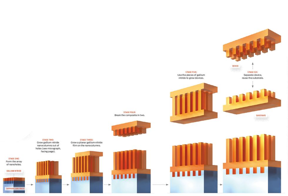
NanoGaN circumvents these problems by taking a substrate, such as sapphire or silicon, depositing a thin film of gallium nitride, forming an array of nanometer-size holes in the surface of the gallium, then growing crystalline gallium nitride layer by layer in the holes. Up grows the crystal in the form of columns, each having a radius in the tens of nanometers.
Now, if you let those columns grow in the standard way, they’d still be plagued with the standard types of defects: edge dislocations perpendicular to the growth direction, screw dislocations parallel to the growth direction, and a combination of these two, called mixed dislocations. The screw types are the real killers because they can propagate right into the device’s core, leading to a reduction in the efficiency, output power, and lifetime of the laser.
Wang and his workers solved the screw-defect problem with a counterintuitive trick: You adjust the growth conditions so as to introduce more edge and mixed dislocations. These defects then cross paths with the screw dislocations, annihilating them. Then, having done that, you can reduce, if not eliminate, the other defects.
With a forest of columns to serve as your foundation, you can build up a film of gallium nitride. Under the right conditions, the film will grow not only up the columns but also out, finally coalescing to form a plane. Because it grows on a material having the same crystalline structure, that planar film will have very little strain in it; with a little more vapor deposition, you can build that film into a good, clean crystal of gallium nitride. When it’s ready, you can pull off a piece of high-quality, freestanding gallium nitride either by breaking the nanocolumns or by etching away a thin, sacrificial aluminum gallium nitride layer you’d built into the structure from the start.
 Photos: Wang Nang Wang
Wang’s technology has clearly been inspired by another technique called epitaxial lateral overgrowth. In that approach, you deposit a layer of silicon dioxide on a gallium nitride surface, then remove some of the silicon dioxide, forming stripes several micrometers wide. Then you grow gallium nitride out of the resulting trenches until it’s level with the silicon dioxide layer, at which point it grows laterally, forming a continuous film.
With Wang’s approach, however, the gallium nitride material above the columns is of superior quality, an improvement because the surface area of the gallium nitride is much greater in the array of nanocolumns than in the more sparsely distributed stripes, he says. Wang believes that because the surface area is much bigger, the growth process has a chance to annihilate a greater proportion of the screw-dislocation defects before they are fixed in the crystal structure.
Laser chip manufacturers can buy NanoGaN’s substrates and just grow their own devices on top of the side that’s covered in the planar film, incorporating everything into the laser diode product. But it would be much better for them if they built their devices on top of the other side of the substrate—the one that has the nanocolumns—so they can then pull off the substrate and return it to NanoGaN, to be refurbished for reuse. To reuse the substrates, you need to polish them: You add a few micrometers of gallium nitride to replenish lost material, poke holes in the surface, and grow new nanocolumns of gallium nitride in them.
Wang estimates that one piece of freestanding gallium nitride could be reused from 60 to 80 times. It’s a big selling point for the company’s technology. Some analysts believe that if we keep chewing up gallium at our current rate, we’ll deplete all known reserves in a decade. That’s a minority view, but pretty much everybody agrees that gallium will probably get scarce sooner rather than later.
The nanocolumn method’s other great advantage is that it lets you make a really thin laser chip. That means you can get more heat out—which extends the chip’s life—and channel more light in the direction you want it to go, to raise efficiency. That’s a boon not only for state-of-the-art lasers but also for plain old LEDs.
And that’s not all: Nanostructured gallium nitride will also make it possible to fabricate LEDs that efficiently emit light in the longer wavelengths of green. LEDs at such wavelengths today are disappointingly dim. The problem occurs in their active regions, where electrons and holes recombine to form light. In all nitride LEDs, the active region is a series of layers of indium gallium nitride, and green light demands a lot of indium. And therein lies the difficulty: It’s hard to get enough indium into the active layer without compromising the quality of the material.
Recently, though, researchers have found that you can get a much brighter green laser by building the LED not along the standard crystalline cross section but rather on a bias. This method exposes one of the semipolar planes, so called because the internal electric field is far weaker, so the chance that electrons will recombine with holes to produce light is greater. But even more important, by growing crystals in this way you can get a lot more indium into the active layer.
Other companies do this by cleaving a gallium nitride crystal along a semipolar plane and growing all the nitride-based layers needed to make a device on the exposed face. NanoGaN instead mills its nanocolumns along the proper angle, exposing a semipolar plane on top of the bias-cut columns. The gallium nitride then grows on top of that plane, producing material that then coalesces to form a corrugated, rather than planar, film. Thanks to the corrugation, Wang believes it will be possible to create devices in which the active layer is three times as big as the one in a conventional LED. The concentration of indium isn’t greater, but the area is. Such a structure should produce a far brighter green light than anything seen yet.
Making dreams come true takes cash—lots of it. But cash is a particularly scarce commodity now. Nevertheless, in February 2008, the University of Bath spin-out secured £250 000 (about $413 000) in seed funding from the university’s commercialization fund, then got twice as much in first-round funding four months later. This past October, NanoGaN shored up its position through its acquisition by a leading specialty substrate company, IQE, in Cardiff, Wales. Wang has become the chief scientific advisor to the company.
To ramp up production as fast as possible, NanoGaN wants, reasonably enough, to replace its home-built HVPE vapor-deposition reactor with an industry-grade version. That’ll take at least six months. Meanwhile, it has joined with another firm that already has such a reactor. Together the two firms should be able to deliver up to 300 substrates per month. By way of comparison, Sumitomo now dominates the industry by producing, according to industry sources, 700 to 1500 substrates per month; a rate of 300 per month would put NanoGaN in second place.
The company has recently simplified its manufacturing method, slashing the number of steps from 12 to 5. “When you reduce the steps you might compromise the yield rate,” explains Wang, “but in our case the yield has improved and the quality has improved.” NanoGaN is also looking to scale up from 2-inch to 4-inch (5-cm to 10-cm) substrates, which would mean they could be used in the more accurate tools used by silicon chipmakers.
In the meantime, potential rivals are working on other technologies for making better GaN substrates. One being pursued by Osaka University, in Japan, and by the manufacturer Ammono, in Poland, involves adding sodium to molten gallium in a nitrogen atmosphere. This technique suffers from the need to coat the reactor with a very expensive platinum liner that’s etched away by the process materials, contaminating the gallium nitride. However, if the kinks can be ironed out, this method could make very high-quality GaN in mass quantities.
Just to be safe, Wang is also looking into this approach, with a partner in Taiwan. Still, he is confident that he has “10 years at least” before any rival technology can threaten him.
Now NanoGaN stands to beat the big boys by grabbing a healthy slice of the burgeoning market for the building blocks of lasers. By increasing the supply of this crucial component in game consoles, video recorders, and a host of other products, the company should help to cut the prices of all these electronic goodies.
This article originally appeared in print as “Crystal Method.”
For all of 2010’s Winners & Losers, visit the special report.
About the Author
Richard Stevenson got a Ph.D. at the University of Cambridge, where he studied compound semiconductors. Then he went into industry and made the things. Now, as a freelance journalist based in Wales, he writes about them. His story on NanoGaN —a feisty start-up headquartered in Bath, England—is the third article he’s written for Spectrum.