
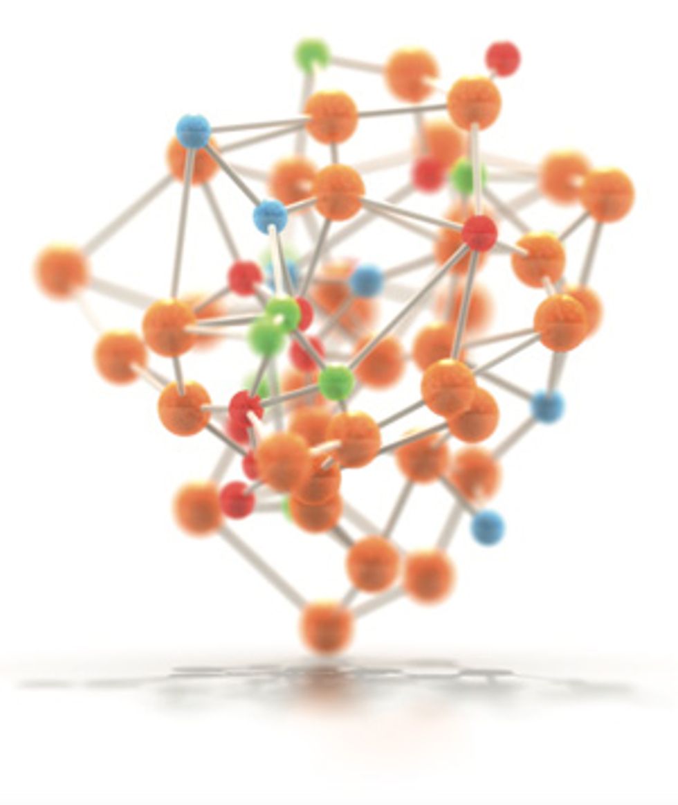
 Illustration: Bryan Christie Design
Amorphous silicon has long been the king of flat-panel displays. It began its reign in PC monitors and high-definition TV, then conquered netbooks, e-readers, and smartphones. No other substance was as suitable for the thin-film transistors that sit behind a display’s hundreds of thousands of pixels, turning each one on or off.
But soon the dominion of amorphous silicon will pass, because it can’t provide what coming generations of electronic products will require. For one thing, it isn’t fast enough. Next-generation LCD TVs will be refreshed at least 240 times a second, which is two to four times as quick as today’s versions; that way, they’ll provide sharper fast-action sports and movies. Three-dimensional displays will need refresh rates twice again as high, to provide all that fast-motion goodness to each eye.
Nor are today’s thin-film transistors stable enough for displays that use the organic light-emitting diode (OLED), a thin, efficient, high-contrast technology. Stability matters because the “threshold voltage” that an amorphous silicon transistor needs to turn on tends to drift as the transistor works. And both the problems of slow switching and drift get worse when amorphous silicon devices are made on flexible plastic, which is a critical design requirement for tomorrow’s roll-up displays. Such displays will enable a laptop-size screen to fold away for storage inside a smartphone.
For these reasons, researchers and display manufacturers need a replacement in hand when the day comes for amorphous silicon to step down from its throne. And they already have their eyes set on a promising heir—in fact, a whole family of materials, known as amorphous oxide semiconductors. They’re amorphous because like today’s silicon standby, they lack a regular crystalline structure, and they’re oxides because they’re made of oxygen compounded with two or three metals, most commonly selected from zinc, indium, gallium, and tin.
Amorphous oxides can form thin films that are transparent and electrically conductive, which is why they already serve as the see-through electrode layer in displays and solar cells. It was this quality that led to the surge in research that began in 1996, when Hideo Hosono and his colleagues at the Tokyo Institute of Technology first noted the merits of amorphous transparent conducting oxides.
We believe that amorphous oxides could do more than simply serve as a passive electrode. They could also replace amorphous silicon as the active semiconducting material that does the heavy lifting as the channel in thin-film transistors.
Here’s what’s great about amorphous oxides: First and foremost, charge can zip through them 20 to 40 times as fast as in amorphous silicon. This speed is defined by a material’s charge-carrier mobility, and the higher it gets, the faster transistors can switch.
Second, unlike amorphous silicon, amorphous oxides can be deposited at low temperatures without compromising their electronic properties. That means they can be laid down or even printed on pliable plastic sheets to make paperlike displays. Such printing could make flexible electronics cheap and ubiquitous. Finally, because the materials are transparent, they could be used in electronic-ink screens that could be laminated on windshields, windows, and eyeglasses.
Even some of the first thin-film transistors made from amorphous oxide semiconductors showed amazing promise. These devices, first reported in November 2004, also by Hosono’s group in Tokyo, consisted of indium gallium zinc oxide (IGZO) built at low temperatures on flexible plastic substrates. They had more than 10 times the charge-carrier mobility of amorphous silicon transistors. Two months later, our research group at Oregon State University reported zinc tin oxide transistors with mobility up to four times as high as that.
Reports on transistors made from zinc indium oxide and many other combinations followed in quick succession. These devices have consistently performed better than their amorphous silicon counterparts.
The advantages of oxide semiconductors over amorphous silicon are causing a stir in the display industry. Just two years after the first oxide-based transistors were reported, Korea’s LG Electronics Co. revealed a prototype OLED display that used IGZO transistors to drive its pixels. Other companies followed quickly with oxide-based displays of their own. Samsung presented a 19-inch OLED and a 17-inch LCD in 2009. AU Optronics Corp., in Taiwan, introduced a 37-inch LCD in early 2010. Samsung followed later that year with a 70-inch ultrahigh-definition (4000 by 2000 pixels) 3-D LCD panel with a 240-hertz refresh rate.
Several companies have also reported flexible displays built on oxide transistor backplane technology. Toppan Printing Co., in Tokyo, made the first black-and-white plastic e-paper displays using oxide transistors in 2005. It has since made an e-paper display measuring 5 centimeters diagonally with a resolution of 160 pixels per centimeter. LG and Dai Nippon Printing Co., also in Tokyo, have reported small, flexible OLED displays fabricated on stainless steel.
Researchers still do not fully understand the materials science or the device physics, but it’s apparent that today’s best IGZO devices would do well in LCD backplanes and are nearly up to the needs of OLED displays. For that latter application, the key question is device stability—that is, the problem of drift in the transistors’ threshold voltage. Recent progress suggests that stability will not be a showstopper.
Of course, the US $100 billion flat-panel display industry has been built on amorphous silicon, and the new materials will have to contend with its 30-year head start. But amorphous silicon is a mature technology; it is extremely unlikely that anyone will overcome the limitations it faces now, because these arise from the material’s fundamental physical and chemical nature.
There’s little doubt that amorphous oxide semiconductors can oust amorphous silicon; the only question is when. The answer depends mainly on how long it will take to develop large-scale manufacturing capability. The oxide thin-film transistor fabrication process is very similar to that used for amorphous silicon devices, so the display industry can leverage much of the existing infrastructure and know-how.
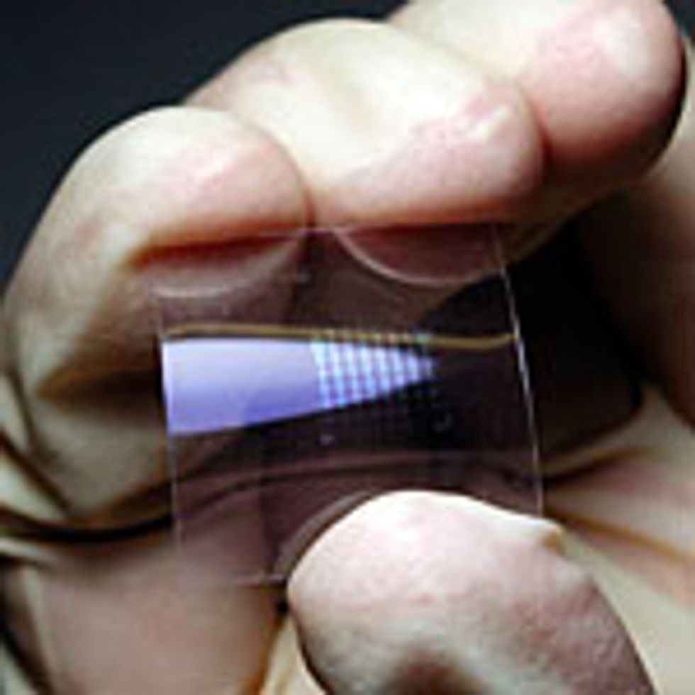
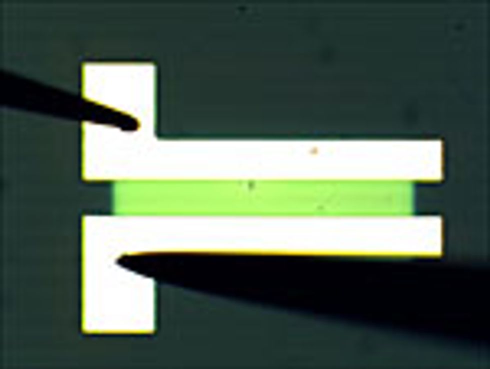
such as this 150-pixel-per-inch resolution black-and-white electronic paper [top] by Japan’s Toppan Printing Co. use amorphous oxide semiconductor thin-film transistors [bottom left], devices that were first reported by researchers at the Tokyo Institute of Technology; at an Oregon State University lab in Corvallis, tests are performed on a single transistor [bottom right].
To understand the promise of amorphous oxide semiconductors, we first have to deconstruct the term. Let’s start with amorphous materials in general and why they are relevant for large-area electronics.
Solids can be crystalline, polycrystalline, or amorphous depending on how their atoms are arranged. In a single crystal the atoms stand in perfect order, forming a repetitive 3-D pattern. In a polycrystalline solid, many microscopic mini crystals, or grains, butt up against one another in a haphazard manner.
In an amorphous solid, each atom and its nearest neighbors stand in a not-quite-perfect order, an arrangement that gets increasingly erratic as you zoom out. The atom’s geometry with respect to its second-nearest neighbors will be less predictable, still more random with its third-nearest, and so on.
The random arrangement of atoms tends to give amorphous materials smooth surfaces and uniform structure when they are produced as a film, which can measure anywhere from tens to hundreds of nanometers thick. And these films are more robust than polycrystalline ones, whose grain boundaries act like shunt paths for impurities. Water vapor, for instance, would more readily penetrate polycrystalline films. That’s why amorphous silicon has wrested the domain of thin-film transistors from crystalline silicon, its electronically superior cousin.
Single-crystal silicon is the unrivaled ruler for integrated circuits used in mainstream electronics, and it has worn its crown since the 1960s. But single crystals are too costly, brittle, and heavy to cover 2-meter-wide glass panels. While thin-film polycrystalline silicon can work well for transistors in large high-performance displays, it requires costly, complex processing.
Amorphous silicon, on the other hand, has just what this job requires. Large glass panels can be cheaply coated with uniform thin films of the stuff at high volumes, producing hundreds of thousands of electronically consistent transistors.
Transistors have three electrodes. A voltage applied to the gate electrode allows charge to flow through a channel between the source and drain electrodes, turning the device on. Like silicon integrated circuits, thin-film transistors are built layer by layer. Films of various materials are coated one over the other on a substrate to form the electrodes and channels. Amorphous silicon films form the semiconducting channel layer in thin-film transistors.
For all its advantages, amorphous silicon really isn’t the best electronic material. That’s because the more randomly you arrange the atoms in a solid, the harder it is for current to flow through. Charge carriers travel in amorphous silicon at only one-thousandth the speed they do in single crystals. In LCD pixel electronics, that speed limit hasn’t mattered much—until now.
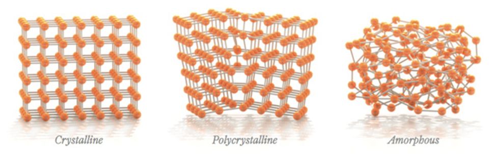 Solid Insight: Atoms line up in an orderly 3-D array in a crystalline solid (left), while a polycrystalline solid (middle) is made of smaller crystalline chunks. In an amorphous solid, perfect order goes out the door: The irregular arrangement lends itself to the formation of smooth, uniform films but also slows down charged particles—a mixed blessing for thin-film transistors.Illustration: Bryan Christie Design
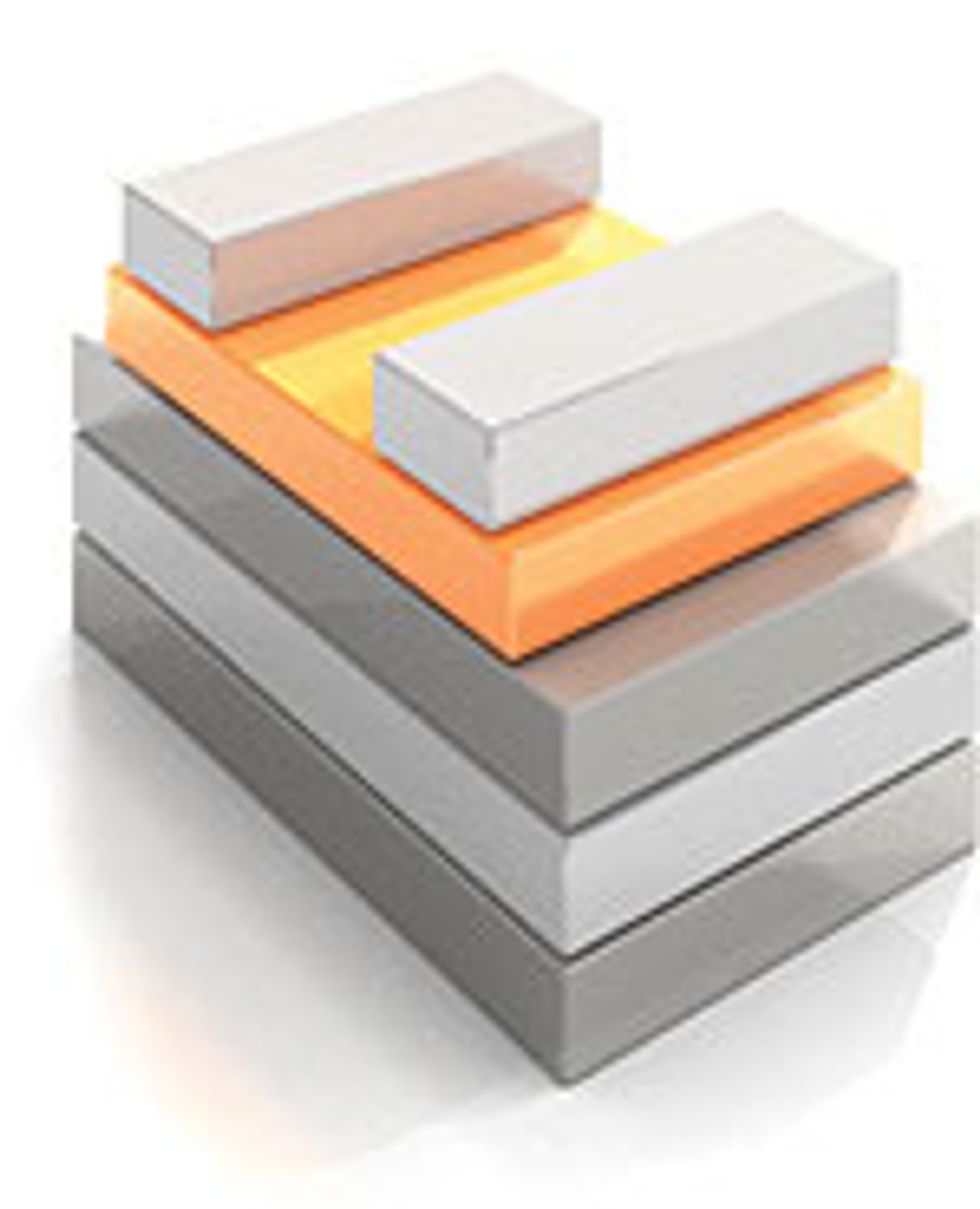
or thin-film transistor, uses an amorphous oxide semiconductor channel [orange] to connect two electrodes—the source and the drain. A voltage applied at a third electrode, the gate, allows charge to flow through the channel, switching on the device.
This is where amorphous oxide semiconductors come in. They offer all the advantages of amorphous silicon for large-scale electronics, with much better electronic properties to boot.
But first, a bit more about these materials. The metal atoms for the oxides are selected from the 15 elements that sit in rows 4 to 6 and columns 11 to 15 of the periodic table. This block includes rare elements like silver and gold as well as environmentally unfriendly ones, like arsenic and lead. Eliminating toxic and costly materials leaves 8 elements that can give 28 dual-oxide combinations.
The individual metal oxides, say, zinc oxide and tin oxide, tend to become polycrystalline when deposited as thin films. But an interesting thing happens when the two are mixed in similar concentrations and deposited. Because they have different crystal structures, the atoms cannot figure out which structure to adopt, and zinc tin oxide ends up as an amorphous film.
A key advantage amorphous oxides hold over amorphous silicon is their higher charge-carrier mobility. Electrons in the oxides fly about in a spherical region around the metal nucleus. The radii of these spherical orbitals are large. So even when atoms are arranged amorphously, neighboring atoms’ orbitals overlap to a large extent. Electrons can therefore rapidly skip between atoms in the solid. In amorphous silicon, by contrast, electrons move around the nucleus in thin dumbbell-shaped regions that don’t overlap much.
The electron-rich amorphous oxide films are conductive. But in order to make effective transistor channels, they must be insulating. They attain that ability when they are deposited in the presence of oxygen, which mops up free electrons. That way almost no current flows in the transistor’s channel unless the proper voltage is applied at the gate.
But when that voltage is applied, the device switches on and the charge flies. In today’s oxide transistors, electrons have a mobility of about 10 to 20 square centimeters per volt-second, as opposed to 0.5 for amorphous silicon transistors. Quicker-moving charges translate to faster, higher-current transistors. That means oxide transistors can carry up to 40 times as much current and switch on and off up to 40 times as fast. Further, if a transistor can carry charge quickly, it can be made smaller, which means more pixels can be packed into a square millimeter as ultrahigh-definition displays require. As research and development progress, we expect to get even higher mobilities.
Another advantage of amorphous oxides presents itself at low process temperatures. Making semiconductor thin films usually requires putting down the vapor form of the material on a substrate, where it solidifies. The higher the process temperature, the better the film’s electrical properties.
Amorphous silicon films are typically deposited at around 300 to 350 °C. These temperatures work for glass, but they would distort plastic. At plastic-friendly temperatures, below around 200 °C, amorphous silicon transistors degrade tremendously.
Amorphous oxide semiconductor films, however, are typically deposited at benign temperatures below 100 °C. Their performance usually improves when they are baked at temperatures of around 250 to 300 °C, but even films processed at room temperature can easily be 10 times as mobile as amorphous silicon. This opens up the possibility of making roll-up electronic circuits on plastic.
What’s more, these oxides can be prepared in liquid form and sprayed onto a surface. If you tried doing that with a silicon-based system, you’d need a vacuum chamber to keep out oxygen, which would combine with the silicon to form silicon oxide, an insulator. But the new materials aren’t degraded by oxygen, because they’re oxides to begin with. These materials could print thin-film transistors on plastic using inexpensive roll-to-roll processing techniques similar to those used to print newspapers.
Some issues must still be solved, beginning with device stability. Oxide-based transistors are more stable than the amorphous silicon kind, but they’re still not as stable as the industry would like. This can be a problem even with LCDs, which are switched on and off by voltage, with a threshold that is not perfectly constant. It’s an even bigger problem with OLEDs, which are switched by current—an arrangement that makes the circuits even more sensitive to transistor stability. We are working with Applied Materials, in Santa Clara, Calif., on ways to make these devices more stable.
Then there’s the problem of printing inexpensive, flexible displays. True, Toppan’s process can do so for e-paper, but these black-and-white displays can get by with slow switching speeds and low power. Roll-up color LCDs and OLEDs require oxide transistors of higher quality.
We are now working with Oregon State chemistry professor Douglas Keszler and Inpria Corp., in Corvallis, Ore. They are designing high-quality IGZO inks as well as other semiconductor and insulator inks. When these inks are used to pattern transistors, the devices perform almost as well as those made using conventional vacuum processes. The next step would be to pair this printing approach with a high-volume roll-to-roll process on flexible plastic substrates.
We are also working on zinc tin oxide, which incorporates less expensive metals and can be more easily fabricated as thin films. The problem is that its electronic properties are harder to control. We are now trying to tame them.
Finally, dare we mention an unrealized dream of ours? We would love to discover a p-type amorphous oxide semiconductor. Unlike today’s amorphous oxides, which juggle electrons and are known as n-type, such a semiconductor would shuttle around positively charged holes—virtual particles corresponding to the absence of an electron.
Complementary metal-oxide semiconductor (CMOS) technology, which combines n- and p-type semiconductors, was a game changer for silicon integrated circuits, making possible low-power computer chips and microprocessors. Having something akin to CMOS for amorphous oxide semiconductors would have the same effect. For now, together with Boeing, we are trying to use n-type oxide transistors in simple digital and analog logic circuits.
Change is afoot: Although no one has announced it formally, recent developments suggest that display industry leaders are ramping up plans for large-scale production. Companies are already making oxide transistor-based displays with sixth-generation LCD panel manufacturing equipment, which uses glass substrates 185 centimeters wide and 150 cm high. What’s more, the scale of recently demonstrated displays suggests that the industry will soon be able to use the eighth-generation equipment that makes today’s large high-performance LCDs. Look for the new materials to begin to appear in commercial displays as early as 2012.
In 2010, Samsung introduced a 14-inch OLED screen that was 40 percent transparent. While the company hasn’t revealed its pixel-controlling technology, there is no doubt that amorphous oxide transistors are perfect for the application and could bring see-through displays into consumer products.
Given the astonishing developments of the past two years, it’s easy to forget that amorphous oxide semiconductors are still in their early adolescence; practical work started only about five years ago. In a few more years, they’ll start appearing in your home, in your hand, and perhaps on the lenses of your glasses.
This article originally appeared in print as “Thin, Fast, and Flexible.”
About the Authors
John F. Wager and Randy Hoffman began working together at Oregon State University. Wager is a professor of electrical engineering and computer science there and the lead author of the 2008 book Transparent Electronics. His student Hoffman—while working toward his master’s in electrical engineering—researched oxide semiconductor–based thin-film transistors, producing the first in a series of key patents. He is now a senior engineer at HP, where he develops oxide-based, printed, and flexible electronics and active-matrix displays.