5 April 2011—At just a few nanometers across, quantum dots are tiny—so tiny that scientists attempting to insert new atoms into their structures have found that the atoms tend to quickly wander back out.
Now an Israel-based team has made these atoms stick, creating the first pairs of p-type and n-type semiconductors, pint-size versions of the building blocks of today’s diodes and transistors. The work could eventually pave the way for new flexible solar cells and LEDs, which would be built from the bottom up.
Adding impurities to a crystal can greatly alter how well a semiconductor conducts electricity. The process has been a basic part of creating semiconductor devices for decades. In principle, this technique, known as doping, could also help manipulate the electronic properties of quantum dots. The tiny semiconductor crystals contain as little as a few hundred atoms, and because their minute dimensions introduce odd quantum effects, some nanocrystals glow at a wavelength of light that’s related to their size. Quantum dots have been used in biology to tag molecules and to image cells, but so far, their utility has been limited because there have been few ways to manipulate their electronic properties without changing their size.
Inserting foreign atoms into the tiny semiconductor crystals could be a powerful way to alter those properties, but until now there has been no good way to do that. You can’t easily dope a wafer of semiconductor and then chop it up to make doped nanocrystals. And slamming charged dopant particles into the crystals, a common process in making doped semiconductors in the chip industry, could easily disrupt the quantum dots’ structure.
Now a team led by Uri Banin and Oded Millo of Hebrew University, in Jerusalem, and Eran Rabani of Tel Aviv University think they have found a controlled way to introduce dopants into quantum dots.
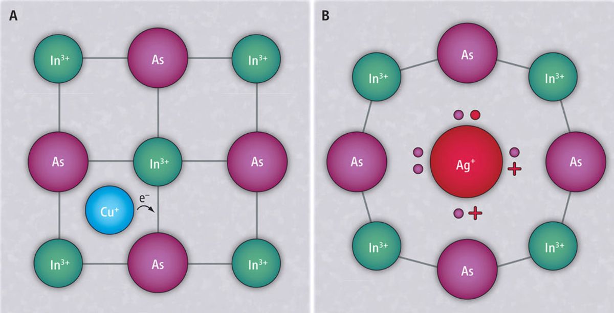
To do so, the group made a solution containing 3.3-nanometer-wide crystals of indium arsenide and either silver or copper atoms. These atoms bounced around in solution due to the random jiggles of Brownian motion and eventually wandered inside the crystals.
The copper atoms lodged themselves into gaps between atoms in the lattice, donating their extra outer electrons to the crystal to create an n-type nanocrystal. Although silver atoms diffused through the crystal at much the same speed, they instead dislodged indium atoms and took over their positions in the lattice. Because the silver atoms had fewer outer electrons than the indium atoms, they created p-type crystals containing electron-craving "holes."
This is not the first time that impurities have been added to nanocrystals. But until now there was always some uncertainty as to whether the doping process actually changed the electronic properties of the quantum dot, says Charles Cao, an associate professor of chemistry at the University of Florida, in Gainesville. "This is the first solid evidence that demonstrates a capability to create n-dope and p-dope semiconductor nanocrystals," he says.
The team confirmed the doping by studying the crystals’ electronic energy levels using a scanning tunneling microscope. They found that the quantum dots’ Fermi levels—energies that relate to the distribution of electrons in a material—had shifted to higher and lower energies, suggesting that the doping was successful. The findings were published on Friday in the journal Science.
In principle, says Banin, it’s now possible to build small electronic devices like diodes and transistors from the bottom up, in solution, for example by depositing p-type nanocrystals on top of a layer of n-type nanocrystals.
One potential application for doped quantum dots is in solar energy. Nanoparticles have been an attractive material for solar cells, because they can be embedded in flexible plastics, and the wavelength of light they absorb can be carefully tuned.
Junctions made of films of n- and p-type nanocrystals could be used to separate charges the same way they are separated in traditional photovoltaics. By making these junctions from scratch, using a bottom-up approach, says Rabani, "we might be able to make them cheaper, and maybe at the end of the road they would also be more efficient."
"Whatever you can do with nanoparticles, you can do with doped nanoparticles, and now you can do even more," Rabani says.

