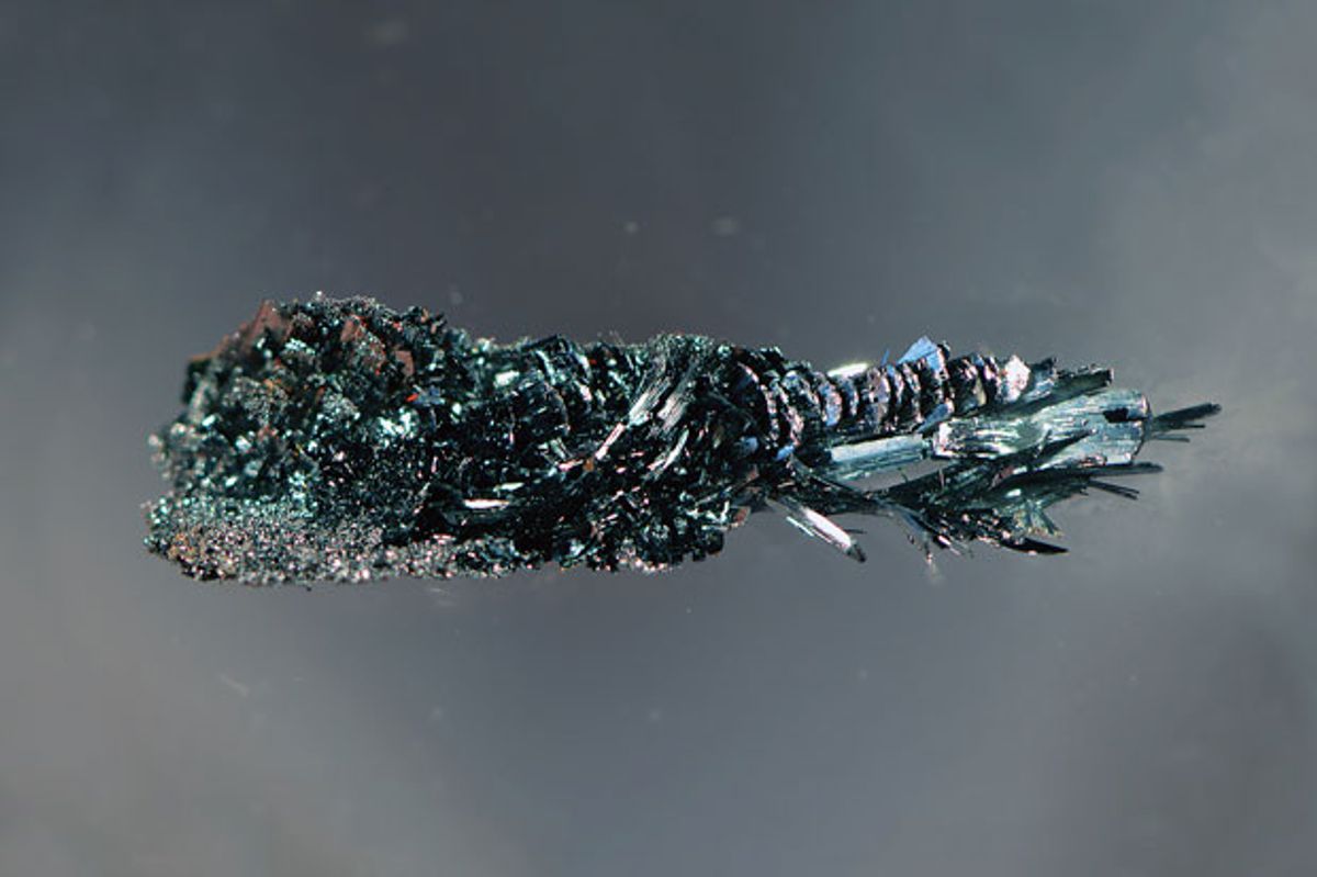
Chemists first synthesized black phosphorus over a hundred years ago. But it was only last year when anybody really took interest in the flaky black stuff. In a series of experiments reported in the first half of 2014, researchers were able to exfoliate black phosphorus into very thin films of only about 10 to 20 atoms thick. Now black phosphorus has become the new darling of two-dimensional materials research and a new hope for a postsilicon world.
The excitement around black phosphorus, which is also called phosphorene in reference to its 2-D cousin graphene, stems mainly from the fact that it has an inherent bandgap, something that graphene lacks. A bandgap, an energy band in which no electron states can exist, is essential for creating the on/off flow of electrons that are needed in digital logic and for the generation of photons for LEDs and lasers.
Black phosphorus doesn’t just have any bandgap. Its bandgap can be fine-tuned by adjusting the number of layers of the material, explains Philip Feng, an assistant professor of electrical engineering and computer science at Case Western Reserve University. His team has demonstrated some of the first black phosphorous mechanical and electronic devices.
The bandgap can be dialed up from 0.3 to 2.0 electron volts. That’s a range covering a regime otherwise unavailable to all other recently discovered 2-D materials. It bridges the bandgaps of graphene (0 eV) and of transition-metal dichalcogenides such as molybdenum disulfide, which range from 1.0 to 2.5 eV.
By combining this bandgap tuning with different choices of contact materials, scientists at Sungkyunkwan University, in South Korea, were recently able to build both n-type transistors—those conducting electrons—and ambipolar transistors, which conduct both holes and electrons. Such a mix brings the material closer to mimicking the complementary logic used in today’s silicon chips.
Scientists are also excited about black phosphorus for photonics, “since optoelectronic functions, including light absorption, emission, and modulation, of semiconductor materials depend on the size of the bandgap,” says Mo Li, a photonics expert at the University of Minnesota. Black phosphorus’s bandgap range means it can absorb and emit light with wavelengths of 0.6 to 4.0 micrometers—covering the visible to infrared. That spectrum could be key to its use in sensors and in optical communications. Li’s group built a black phosphorous photodetector that was able to convert 3 gigabits per second of optical data to electronic signals.
Another cool property, Feng points out, is that black phosphorus possesses an intrinsic, strong in-plane anisotropy, which means its properties are dependent on the direction of the crystal. “This in-plane anisotropy is not readily found in other 2-D crystals derived from layered materials,” he says. His team recently demonstrated the first black phosphorous high-frequency nanoelectromechanical systems resonator. The resonator took advantage of the material’s in-plane anisotropy to generate new elastic behaviors and frequency scaling abilities.
Unfortunately, black phosphorus is hard to make and hard to keep. Currently, it’s made by treating an amorphous form of the element called red phosphorus with high pressure (1 gigapascal) and high temperature (1,000 °C). The resulting millimeter-scale crystals are then exfoliated into atoms-thick flakes for making nanostructures and nanoscale devices.
More troubling is that “when exposed in air, black phosphorous film degrades within a few hours, due to reaction with water vapor and oxygen in air,” explains Li. “Luckily, many inert materials can be used as passivation to preserve black phosphorous devices for weeks or longer.”
If the manufacturing and preservation problems can be solved, perhaps silicon could finally fade to black.
