
Since the invention of the integrated circuit in 1958, the number of processing steps required to make one has grown from less than 10 to several hundreds. At the same time, the silicon wafers on which the ICs are produced have gone from being coin-sized to being dinner-plate-sized.
Today, one of these 300-millimeter wafers can yield more than 700 ICs. And that, for a growing number of chip makers, is precisely the problem. With such a large number of ICs coming from a single wafer and with wafers coming off manufacturing lines at rates of tens of thousands a month, companies can quickly find themselves suffering from chip glut, especially in turbulent markets.
For the past five years, since the bursting of the dot-com bubble in 2000 sent semiconductor sales into a tailspin, the industry has been struggling to rid itself of excess inventory. In the second quarter of 2001, the entire supply chain, including chip makers, distributors, contract manufacturers, and consumer-product manufacturers, was stuffed with an excess of chips worth more than US $13 billion, according to some estimates. Companies stopped hiring new employees and laid off existing ones. As a result, semiconductor industry jobs in the United States alone dropped from 268 000 in 1999 to 235 100 in July 2003, according to the U.S. Department of Labor. As recently as the third quarter of last year, chip oversupply was still at a worrisome $1.6 billion, according to a preliminary analysis by iSuppli Corp., a research firm in El Segundo, Calif. [See graph, "Swimming in Chips."]

Clearly, the semiconductor industry is still facing serious problems as it claws its way back toward profitability and sustained employment growth. And for economic and technological reasons, the relentless drive toward faster, cheaper, and smaller chips is a growing problem. The solution, we believe, lies in a fundamental change in the machines that process the wafers: a switch from batch to single-wafer manufacturing.
The single-wafer approach is a completely serial one, in which just one wafer is processed at a time, all the way through the factory from start to finish. There is never a time when the machines work on a large batch of wafers at the same time, as they do today. The single-wafer technique will solve the oversupply problem by shortening the time it takes to make a finished, packaged chip to less than one month, rather than the three months or more that is typical today. Basically, with single-wafer manufacturing, semiconductor companies will be able to produce chips quickly when the orders come in, in the exact quantities specified by those orders. There will be no need to build up huge inventories that may just sit on shelves until they become obsolete.
And it isn’t just boutique chips, which are made in small quantities, that would benefit from the single-wafer approach. Even commodities like static random-access memory (SRAM) and microcontroller chips, which suffer from periodic oversupply and the resulting price plunges and reduced profits, would benefit from a more agile response to changing market demands.
So what will it take to shift to single-wafer manufacturing? First, consider today’s typical semiconductor plant. It combines single- and batch-processing steps; some of the machines process wafers in groups, while others already process them singly. True single-wafer manufacturing eliminates all the batch processes and uses only machines that process wafers one at a time. Today, only a few semiconductor plants have switched over completely to single-wafer manufacturing.
In 2001, Trecenti Technologies Inc. of Hitachinaka, Japan (now part of Renesas Technology Corp.), adopted 100 percent single-wafer processing for the fabrication of advanced semiconductor ICs on 300-mm wafers. The company’s experience with this technique has been remarkable. It has found that it can reduce manufacturing time from 90 to 30 days, and the number of days needed for each chip layer has dropped from 2.25 to 0.25. Even more remarkable is the improvement in the fabrication time for a wafer of SRAM chips made up of 130-nanometer structures. That time has dropped from about 60 days to fewer than six days.
Several other IC manufacturers are also currently considering 100 percent single-wafer processing. Freescale, Philips, and STMicroelectronics have formed the Crolles2 Alliance. Its 300-mm wafer facility, in Crolles, France, uses single-wafer processing for most steps. Tokyo-based Toshiba Corp.’s minifab, in Oita City, Japan, is another example of IC manufacturing dominated by single-wafer processing.
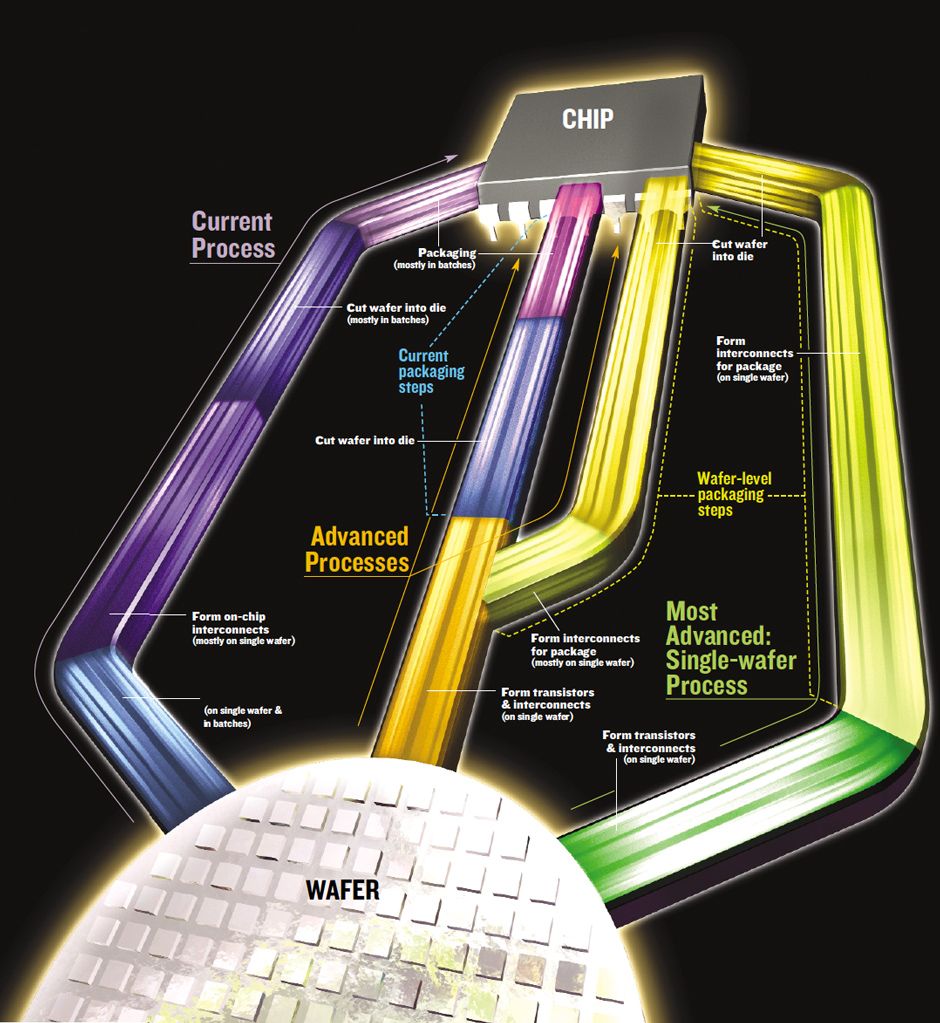
The fabrication of a finished, packaged IC has three key groups of processing steps, regardless of whether it happens in a conventional or a single-wafer setup. First, the transistors are made; next, they’re wired together into circuits on the chip; and finally, the small slivers of silicon, known as die, are packaged into finished chips [see illustration, "Once and Future Process"].
Making transistors, described simply, is a sequential process that builds the four major transistor components: the source, drain, channel, and gate. Basically, the first step in the formation of the transistor is to coat a silicon wafer with a photosensitive material, called a photoresist. The photoresist is exposed to light in the pattern of the areas in which transistors are to be built. Each of these regions will eventually contain the transistor’s four components.
The pattern forms when the light passes through a glass mask patterned with chrome. The exposure of the photoresist to light changes its solubility, so when the wafer is rinsed after exposure, some of the photoresist washes away. What remains is the pattern of transistor areas in photoresist on the wafer. This step, called lithography, is repeated at almost every stage of manufacturing, building up the transistors, and therefore the chip, layer by layer.
Next comes a step called ion implantation, which infuses the wafer with certain ions, typically arsenic or boron, in the areas where the photoresist has been removed. These ions are called dopants, because their presence changes the transistor’s electrical properties, for example, its resistance or the voltage that must be applied to the gate to turn it on.
The next task is to build the gate. A thin layer of silicon dioxide insulation is grown to electrically isolate the gate from the channel. This step typically occurs in a large furnace that heats the wafers in an oxygen-rich environment. The top of the layer is infused with nitrogen to provide a physical barrier to the passage of impurities from the gate into the silicon dioxide. Then polycrystalline silicon is deposited over the entire wafer.
The next step takes the wafer back to lithography, where the same process of exposure of photoresist through a mask, followed by rinsing, leaves photoresist covering the regions where the transistors’ gates are to reside. The lithographic step is followed by an etching step, in which ions, bombarding the polycrystalline silicon surface, wear away all the polycrystalline silicon material not covered with photoresist. The polycrystalline silicon gates remain after the protective layer of photoresist is removed.
After gate formation comes another ion-implanting step, this time to adjust the electrical properties of the source and drain, and then annealing, in which the wafer goes either back into the furnace or into a single-wafer annealing machine, enabling the ions to move into the proper locations in the material.
Making the wires that connect the transistors into circuits is the final step in the formation of the ICs on the wafer. The chip may have as many as nine levels of wires, which are all formed the same way. First an insulating material is deposited onto the tops of the completed transistors. Then trenches are etched into the insulator and filled to overflowing with metal—usually tungsten or copper. Polishers grind down the metal until it is level with the top of the insulation. These metal structures form the links, or vias, that will connect the wiring to the transistors. A second layer of insulation is deposited on top of the vias, and it too is etched into the desired wire pattern. Then copper is deposited and polished down to be even with the second layer of insulation, forming the first level of metal wiring. This process, called chemical-mechanical polishing, uses both physical grinding and a solution of chemicals to grind the metal to the right level.
Once the circuits are completely built, the wafer moves on to testing and packaging. For packaging, the wafer is sliced up into individual die. The chip is enclosed in an airtight package, with electrical pads on the die connected to the familiar leads protruding from the package.
In today’s typical fab facility, the single-wafer steps include lithography, chemical-mechanical polishing, and the material deposition used in wiring the transistors. But some thermal processing steps, like silicon dioxide growth, the infusion of nitride into the gate insulation, and annealing are done in batches of as many as 200 wafers in large furnaces. Periodically, throughout manufacturing, the wafers need a cleaning to clear away debris that may have accumulated during previous manufacturing steps. Some of the cleaning steps dip the wafers into a wet bench, a reservoir filled with a cleaning liquid. Wet benches also handle wafers in large batches.
The batch-processing equipment vastly increases the time it takes for a wafer to pass through the production line. The reason for the delay is that the furnace or wet bench cannot process a single wafer—or even two, or 20—when it arrives from a previous manufacturing step. The equipment’s temperature, gas-flow rate, or chemical concentration is set to handle many wafers at once. To handle fewer wafers would require different settings. So a wafer must wait until dozens of other wafers are ready to go in. This constraint means that some wafers may wait around for days before they move into the equipment for the next step.
The greatest technical advantage of single-wafer manufacturing is that it produces wafers with more good chips than batch processing does. It also produces ICs that are faster and more reliable. There are several reasons for these improvements, but the most important ones can be summed up in two words: tighter tolerances. Single-wafer equipment is smaller than batch equipment, so it is possible to have better control over conditions like temperature and gas flow. In batch furnaces, for example, the annealing temperature or gas flow may vary from place to place inside the furnace. These differences create variations in the electrical properties of the circuits from wafer to wafer, across a single wafer, and even on an individual IC. And these properties, in turn, affect how the circuits work. For example, if the voltage at which the transistor turns on is too high, the transistor switches more slowly than one with a lower threshold voltage. And slower transistors mean slower circuits.
If threshold voltages vary from wafer to wafer, the circuits on those wafers will run at different speeds. And, even worse, if the threshold voltages stray too far from their nominal values, the circuit may not work at all.
The trick in single-wafer manufacturing is to devise processes that handle a single wafer efficiently enough to compensate—through speed, for example—for the economies of scale that are lost with the elimination of batch processing. In the annealing step, for example, the single-wafer alternative to batch processing is rapid thermal processing. It occurs in a chamber in which lamps heat the wafer directly, so the temperature to which each wafer rises is more uniform over time, and the electrical properties of the circuits are more uniform as well.
To speed the wafers through a single-wafer facility, engineers cluster several manufacturing steps into a single unit, which also helps to control ambient conditions more precisely. For example, forming the layers that make up the transistor’s gate takes three separate substeps: growing of the silicon dioxide gate insulation, adding nitrogen to the silicon dioxide to protect the insulation against the infusion of impurities from the gate material, and depositing the polycrystalline silicon that will eventually form the gates of individual transistors. In a single-wafer facility, all three of these substeps can occur inside a single machine, as they do at most of the 47 facilities in the world where the most advanced commercial chips are fabricated.
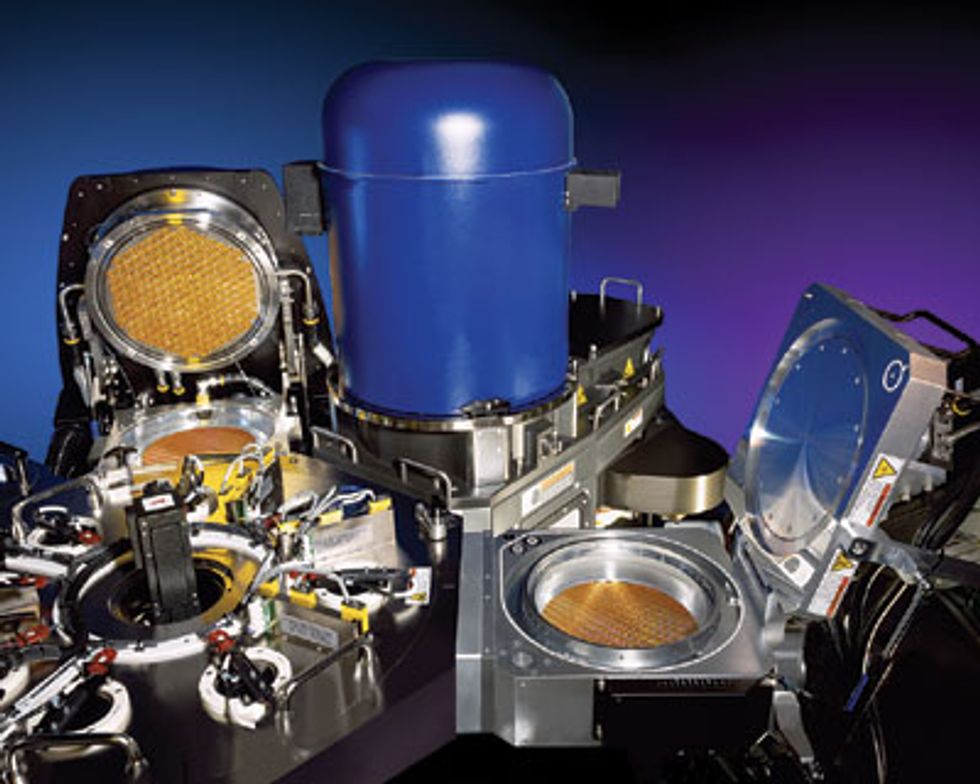 Get it Together: The Applied Centura Gate Stack cluster equipment from Applied Materials consists of separate chambers for making the transistor gate. Each chamber performs a different step in the process—from the growth of the silicon dioxide gate insulation to the deposition of the polycrystalline gate material.Photo: Applied Materials Inc.
These combined machines, known as cluster tools, include a separate chamber for each of the steps of the process [see photo, "Get It Together"]. The wafer passes from one chamber to the next through a vacuum region located at the center of the unit. Connecting the process chambers through a vacuum prevents the surface of the wafer from being exposed to the atmosphere, which could contaminate it, throughout the entire gate-formation process.
The extreme isolation available with this cluster machine allows the silicon dioxide thickness to be controlled uniformly to a few monolayers of atoms—a control not possible with batch machines. Such uniformity is critical to the fabrication of the most advanced circuits today—those with wires only 90 nm across—because the total thickness of the silicon dioxide layer that insulates the gate from the channel in these devices is only 1 or 2 nm thick. Cluster equipment will become even more critical in the next semiconductor generation, which will produce wires only about 65 nm wide.
In some cases a single-wafer machine is fundamentally better than its batch counterpart because of differences in the physical principles through which they work. For example, both the rapid-thermal-processing machines used in single-wafer manufacturing and the furnaces used for batch processing heat the wafers by irradiating them with photons. But the wavelengths of the photons in the two processes are different. The batch-processing furnace produces only photons with wavelengths above 800 nm—in the infrared region of the optical spectrum.
The single-wafer alternative, on the other hand, uses rapid-thermal-processing lamps that produce photons both above and well below 800 nm—even some photons in the visible and ultraviolet parts of the spectrum. These shorter-wavelength photons are more energetic than the infrared photons and can excite the atoms of the wafer electronically. As a result, they permit a lower processing temperature while nevertheless shortening the processing time from hours to minutes. The lower temperatures also make it easier to introduce new materials into the manufacturing process, for example, new gate insulators that will lower the leakage current between the gate and the channel and cut down considerably on the power that the ICs consume. The bottom line is improved performance, reliability, and yield for the chips.
Another attractive feature of single-wafer processing equipment is the use of sensors inside the machines to measure important parameters, such as wafer temperatures, gas densities, and reaction rates. These sensors relay information to a database and allow software to adjust, in real time, any parameters that may have strayed from their nominal values.
Batch equipment, on the other hand, uses monitor wafers that run either ahead of or alongside the circuit wafers. On these monitor wafers are circuits that allow engineers to measure line widths, line spacings, wire resistances, and other circuit features. After the process step ends, the monitor wafers are taken out and their various circuits are measured. Engineers use the information to make adjustments for the next batch of wafers to move through that piece of equipment.
Some single-wafer processing steps, notably lithography, also use monitor wafers. But the sensors used in other single-wafer steps let technicians make adjustments to properties like wafer temperatures and gas concentrations on the fly. It gives them better control of manufacturing conditions and yields wafers with less variation from chip to chip and from wafer to wafer.
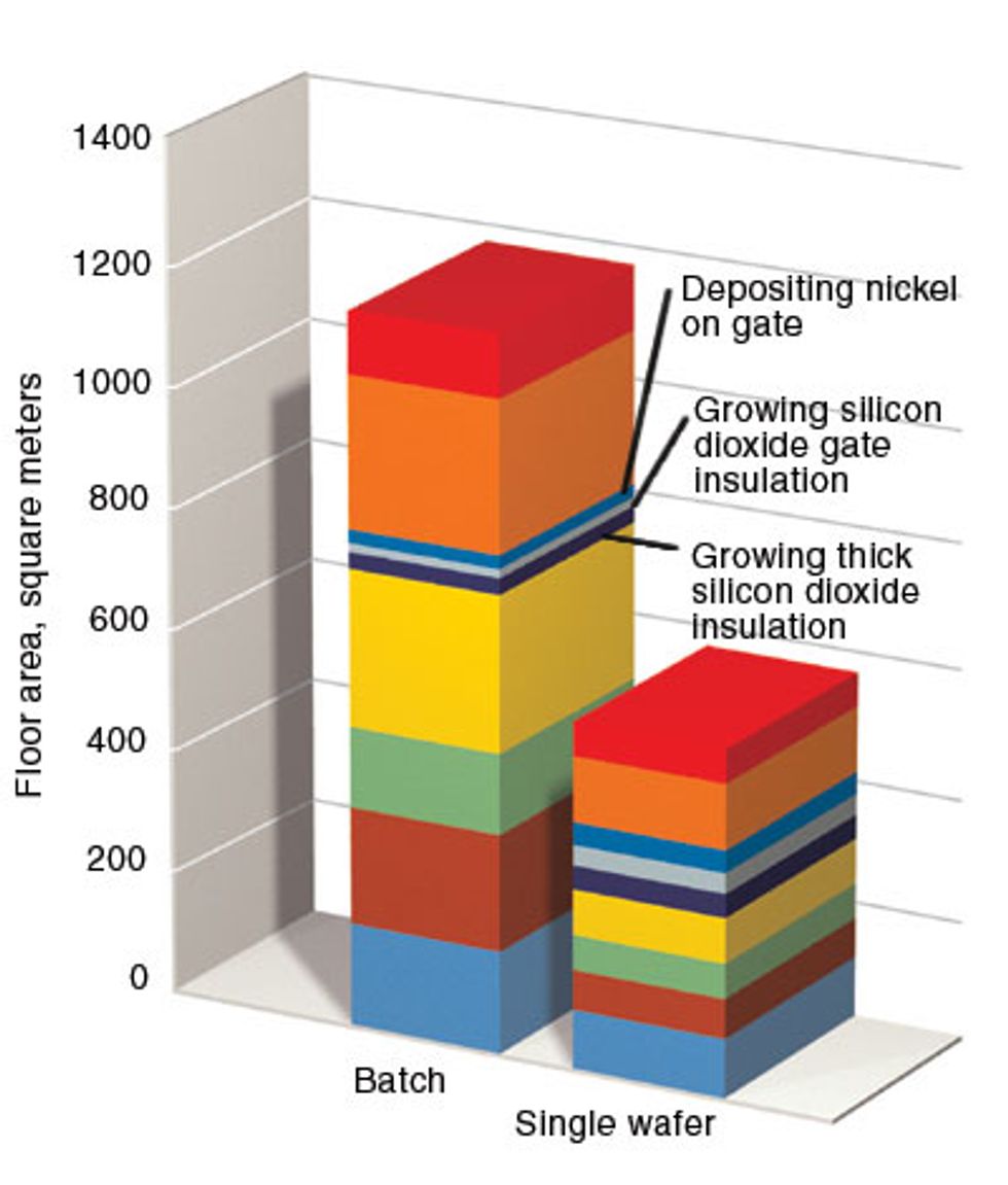 Saving Space: Single-wafer equipment takes up half as much floor space as batch equipment. In an era when the cost of a wafer fab runs in excess of US $2 billion, a smaller fab can mean lower construction and maintenance expenses.Illustration: John MacNeill
The economic advantages of single-wafer processing extend beyond the chips themselves. Even the equipment itself is much smaller physically than that used in batch processing. For example, a state-of-the-art facility that produces ICs on 300-mm wafers and produces 25 000 wafers per month might occupy 10 000 to 20 000 square meters of floor space. Of that area, batch-processing equipment would take up 1200 m2. The area taken up by the equivalent single-wafer processing equipment is only 600 m2 [see graph, "Saving Space"]. The smaller area means that building the facility costs less, and many operating expenses—such as lights, air purification, and temperature control—also are significantly lower. The equipment itself costs slightly less as well—about 6 percent less—for single-wafer processing than for batch processing, but that 6 percent represents millions of dollars. In an era when it costs between $2 billion and $3 billion to build a semiconductor manufacturing plant, even a savings of a few percent matters.
Single-Wafer Processes are becoming important in packaging chips as well as in building the wafers. Today many packaging operations still use large wet benches to clean debris—small particles of wiring metal or insulation—from the surface of large batches of wafers. But fab facilities—particularly advanced ones—are increasingly turning to single-wafer cleaning equipment for the packaging process. The leading manufacturer of single-wafer cleaning equipment is The Sez Group, Zurich, Switzerland. Applied Materials Inc., Santa Clara, Calif., also offers a machine for cleaning individual wafers during transistor formation.
A packaging technique called wafer-level packaging is increasingly common among chip makers. It is a step toward single-wafer processing, because it makes it possible to do the cleaning steps and to build connections between the package and the chip, and among chips in the package, in a single-wafer fabrication facility. It may seem obvious enough, but in fact this bucks tradition in the industry; most wafers today are shipped to remote locations for packaging, which can add weeks to the manufacturing process.
To sum up, the three main business advantages of single-wafer processing—faster time to market, smaller inventory, and lower manufacturing cost—are starting to improve chip makers’ ability to manage their supply chains and better deal with the boom and bust cycles that have long plagued the industry.
Faster time to market is possible because it takes less time for wafers to make it through the fabrication process. The three months it takes to make a wafer full of chips with batch-process equipment can be reduced to less than a month with a pure, or nearly pure, single-wafer setup.
For chip makers, these advances are overdue. The glut of memory and logic chips that even now continues to affect the market can be blamed, at least in part, on making wafers in large batches. This perennial chip overabundance has long depressed chip prices. So while the number of chips sold in the first three years of this decade climbed steadily from 300 billion in 2001 to 360 billion in 2003, revenues stayed relatively flat, at about $160 billion per year. In other words, manufacturers have been selling more chips, but they have not been making any more money [see graph, "Where It Hurts"].
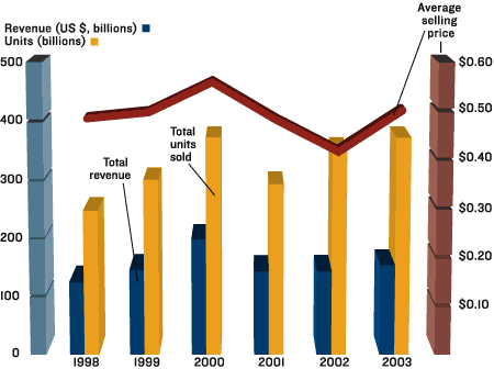 Where It Hurts: In 2001, the IC industry suffered the devastating effects of the bursting dot-com bubble. Revenues were lower (blue bars) and fewer units were sold (yellow bars). But even though the number of units sold began to climb again in 2002, revenues did not follow suit, largely because of a drop in the average selling price per chip (red), caused by an oversupply.Source: In-Stat/MDR
This past year of 2004 saw some good news for the industry: record-breaking revenue of $214 billion—28 percent higher than that of 2003, according to the Semiconductor Industry Association, in San Jose, Calif. But the bad news is that revenues will not grow significantly in 2005. Chip prices are again dropping because of chip oversupply. In a report published in November 2004, iSuppli analysts predicted that 2005 chip prices would fall in most categories of ICs, from memory chips to standard logic circuits.
The complexity of IC manufacture grows with each new generation of semiconductor technology. On-chip wire widths shrink. New techniques and new materials, both insulators and conductors, come into the mix. The cost of building a semiconductor fabrication facility continues to skyrocket. Before too long, single-wafer manufacturing will not be merely an alternative, it will be a necessity. We believe that within three to five years all manufacturers will be using single-wafer processing exclusively to make transistors and interconnecting wires. They will inevitably adopt single-wafer packaging universally in the following years.
About the Authors
Rajendra Singh (F) is the D. Houser Banks Professor of Electrical and Computer Engineering and the director of the Center for Silicon Nanoelectronics at Clemson University, in South Carolina (srajend@clemson.edu).
Randhir Thakur (SM) is group vice president and general manager of Applied Materials Inc.’s Front End Products Business Group, in Santa Clara, Calif. (Randhir_thakur@amat.com).
To Probe Further
“Special Section on Single-wafer Manufacturing in Nanochip Era,” by Rajendra Singh et al., in IEEE Transactions on Semiconductor Manufacturing, Vol. 16, May 2003, pp. 90-178, gives technical details of the single-wafer approach.
“Dominant Role of Single Wafer Manufacturing in Providing Sustained Growth of the Semiconductor Industry,” by Rajendra Singh et al., in Semiconductor Fabtech, 19th edition (Henley Publishing, London), 2003, pp. 85-93, describes the importance of single-wafer manufacturing.
In “Limits of Integrated Circuit Manufacturing,” Proceedings of the IEEE, Vol. 89, March 2001, pp. 375-93, Robert Doering and Yoshio Nishi explore the processing pitfalls of semiconductor manufacturing.