
My wife recently gained a new appreciation for my work. She was trying to transfer family videos from old videocassettes to DVDs using various gadgets and software running on her laptop. Inevitably, though, the process always yielded a blank screen somewhere in the recording. These interruptions occurred because the laptop kept overheating. Only after she placed it on a stack of books with a fan blowing directly on it could the computer handle the job.
Heat is one of the worst enemies of electronics. Sit on the sofa with your laptop and you quickly feel the heat on your lap. Often though, overheating can be hard to diagnose. You may notice random errors occurring no matter what program you’re running. This is especially true if you use your computer to play advanced video games, which can really tax the microprocessor and the graphics card. If your machine frequently experiences fatal errors or “the blue screen of death” on such occasions, chances are it has thermal management problems. And overheating doesn’t just degrade a computer’s performance; it can also shorten its useful life.
The electronics industry has tended to deal with overheating more at the system level—using cooling fans, for instance, to regulate rising temperatures inside computers. Until recently, heat was not considered a major problem to be addressed in the design of the ICs themselves. But higher circuit densities and faster clock speeds are making chips run so hot that manufacturers can no longer ignore the problem. According to the International Technology Roadmap for Semiconductors (ITRS), which reflects a consensus of chip manufacturers worldwide, managing heat generation within ICs will be a crucial issue in developing the next generation of electronics. Growing concern has in turn sparked new research into chip designs and novel materials that would allow electronics to run much cooler, thereby improving their performance and extending their life span.
Heat is an unavoidable by-product when operating any electronic device. Electronic circuits contain many sources of heat, including the millions and even billions of transistors that are routinely packed into modern ICs as well as the interconnects—the labyrinthine connections linking these components together. In the past, packaging engineers, not chip designers, were the ones who dealt with overheating. They would position components so that any excess heat would move first from the die to a heat sink, and then they’d use a flow of air—from a cooling fan, say—to dissipate heat into the surroundings. Still running too hot? Just use a bigger fan. For years, such coping strategies were sufficient. But now, with the electronics industry aggressively shrinking chip features below 50 nanometers and moving toward three-dimensional integrated circuits, the era of the big-fan solution has passed.
One good way to assess a microprocessor’s propensity to heat up is by looking at its thermal design power (TDP), which represents the maximum sustained power that must be dissipated when the chip is performing a typical task. With each new generation of microprocessor, the TDP has grown. In the first Pentiums, for example, the TDP was below 20 watts; in the Pentium 4 it reached 90 W. The transition from single-core microprocessors to multicore microprocessors partially addresses the escalating TDP and worsening thermal-management issues, as the new multicore chips gain performance not by increasing clock frequencies but by adding processors. But other big heat issues remain, including the appearance of hot spots within the chip, where heat fluxes can climb as high as 1000 W per square centimeter. What’s worse, according to ITRS projections, within the next five years, up to 80 percent of microprocessor power will be consumed by interconnect wiring in regions of the chips that are particularly difficult to cool.
Designs intended to improve performance in state-of-the-art ICs can also unintentionally aggravate overheating. For example, the silicon-on-insulator technology used in some advanced chips incorporates buried layers of silicon dioxide to boost transistor speeds and reduce power consumption. But the thermal conductivity of SiO2 is only one-tenth to one-hundredth that of regular silicon substrates. And that diminished ability to conduct heat translates into faster temperature rise and earlier device failure.
Three-dimensional electronics, which are currently under development, likewise pose a real nightmare for heat removal. Compared with conventional, 2-D designs, ICs containing stacked dies promise higher integration density, lower interconnection complexity, and a smaller chip area. Researchers are considering various 3-D architectures, but they all share one thing: They are hard to keep cool. Any theoretical performance gain from 3-D electronics will be impossible to realize if thermal issues aren’t addressed. Simulations show that a rise of 10°C in the operating temperature of such an IC increases circuit delay by about 5 percent; doubling the heat density degrades performance by more than 30 percent.
Some of the thermal phenomena taking place in newer chips have never been observed before. For example, a material’s thermal conductivity can change when it is formed into a nanostructure. To understand why, you need to know a little bit about what’s going on at the atomic scale.
Most of the heat conduction in semiconductors (such as silicon) and electrical insulators (such as silicon dioxide) takes place by virtue of the vibrational motion of atoms in the crystal lattices of these materials. These complicated vibrations can be reduced to quantized modes, known as phonons, which in many ways resemble elemental particles. A given material can be characterized by the average distance that the phonons will travel in it at a given temperature. In silicon at room temperature, phonons travel around 50 to 100 nanometers. But if the device’s features are on the order of 50 nm—as they already are in state-of-the-art microprocessors—the phonons will be subject to additional scattering at the boundaries and interfaces inside the chip, which in turn decreases the chip’s ability to shed heat.
As device features approach just a few nanometers, the behavior of phonons gets even more interesting. In such cases, the phonons become spatially confined between layers of different materials and exhibit properties different from those in bulk crystals. While this confinement may prove problematic in many instances, it may also lead to new opportunities to improve device performance, by allowing the transport of the phonons to be precisely controlled and engineered.
These and other factors have led engineers to search for innovative ways to remove heat from electronic devices. One promising approach is to incorporate materials that have a high thermal conductivity into the chip. These can be used as fundamental building blocks for the electronics, or they can serve as specialized heat spreaders, which as their name implies help to move heat so that it doesn’t concentrate and form a hot spot.
Two candidates for such applications are diamond and carbon nanotubes. Diamond, with a room-temperature thermal conductivity in the range of 1000 to 2200 W per meter per kelvin, is the best thermal conductor among bulk crystals and has been considered for use in heat spreaders and in composite silicon-diamond substrates. The room-temperature thermal conductivity of carbon nanotubes is even higher than that of diamonds: around 3000 to 3500 W/m•K. Because carbon nanotubes are also excellent electrical conductors, researchers are exploring using them as transistor channels and interconnects and as thermal vias, which are channels used to move heat vertically through the layers of a chip or a 3-D stack to the heat sinks above or below.
Potentially better than either diamond or carbon nanotubes is graphene, which is a one-atom-thick sheet of carbon arranged in a honeycomb lattice. The material exhibits unique electrical properties. In particular, it has extremely high electron mobility at room temperature. Electron mobility defines how easily an applied electric field moves the electrons in a given material. Higher mobility translates into faster devices.
The first freestanding graphene was produced in 2004, when a research team from the University of Manchester, in England, and the Institute for Microelectronics Technology, in Chernogolovka, Russia, used Scotch tape to peel off a single layer of carbon atoms from a sample of bulk graphite. Since then, the investigation of this material’s unique properties has grown at an astonishing pace worldwide.
Researchers have proposed using graphene in carbon or hybrid silicon-carbon electronics and in ultrasensitive detectors. The new material could avoid many of the challenges that carbon nanotubes face. For one, its planar geometry means that it’s much easier to grow or deposit on a substrate, to pattern or coat with other materials, and to make electrical contacts to. Already, research groups at the University of Manchester, Columbia University, IBM, and elsewhere have succeeded in fabricating field-effect transistors (FETs) from single and multiple layers of graphene. My group at the University of California, Riverside, in collaboration with researchers at Rensselaer Polytechnic Institute, as well as an independent group of researchers at IBM, have experimentally demonstrated that graphene FETs are less noisy—that is, they produce clearer signals—than their carbon-nanotube counterparts and can operate within the strict noise limits for data processing and communication applications.
Although graphene still has significant drawbacks, including the lack of a commercial manufacturing method, its potential as an electronic material looks promising. Recent developments suggest that it may also aid with thermal management. Last year, my group in the electrical engineering department at UC Riverside teamed up with researchers from the physics department to carry out the first measurements of the material’s thermal conductivity and found it to be above 3000 W/m•K near room temperature—higher than that of diamond and on a par with that of carbon nanotubes [see sidebar, "Heating Up Graphene"].
Impressed by such high values, we then set out to find a theoretical explanation. It turns out that physicist Paul G. Klemens, an emeritus professor at the University of Connecticut, had already suggested a theory. Back in 2000, well before all the recent excitement about graphene had begun, Klemens had predicted that graphene would have a higher thermal conductivity than bulk graphite, provided the graphene sheet is large enough. In simple language, this happens because the low-energy phonons, which transfer the bulk of the heat, scatter less in a 2-D system like graphene than in a 3-D stack of graphite. In an ideal, pure sample of graphene, the phonons’ travel distance would be limited only by the size of the graphene flake. Building on this and other work, we then developed our own detailed theory that takes into account the new data on graphene and explains why its thermal conductivity is so sensitive to the width of the graphene flake.
Graphene could be used in a number of ways to dissipate heat. For instance, it would work better than carbon nanotubes for making heat-dissipating, electrically conducting interconnects between transistors. Used as a heat spreader in a 3-D chip, it could be paired with thermal vias made of carbon fiber or carbon nanotubes. In situations where graphene’s high electrical conductivity would prove a problem, it could be combined with an unconventional electrical insulator like synthetic diamond. If necessary, graphene can be converted into an electrical insulator by irradiating it with low-energy electrons.
In short, incorporating graphene into chip designs could yield devices that are faster, less noisy, and run cooler. Of course, the usefulness of graphene—or, for that matter, of diamond or carbon nanotubes—will depend not just on their physical characteristics but also on their cost and their compatibility with existing chip-manufacturing technology. It’s also possible that the high thermal conductivity of graphene may decrease when it is embedded between layers of other materials or when the number of atomic layers gets too high. The exact extent of such changes is a matter of ongoing research. Still, the results so far provide reasons to be optimistic about graphene.
Managing heat in a nanoscale device becomes even more complex as chip designers continue to boost IC speeds while shrinking transistor channels. The relentless push of Moore’s Law, which holds that the number of transistors per chip doubles roughly every 18 months, has led to ever higher speeds and drive currents and ever smaller chip features.
The speed and current limits of a chip are proportional to the electron mobility of the semiconductor materials used in its construction. In silicon at room temperature, electron mobility is mainly limited by phonons, which cause the electrons to scatter. A higher electron mobility usually corresponds to weaker electron-phonon interactions and thus less heat generation.
But efforts to increase electron mobility—and thus the speed and current a device can handle—can end up degrading the device’s ability to dissipate heat. One approach, already used in conventional chips, is to create strain in the atomic lattice of the semiconductor substrate by forming it out of two materials with slightly mismatched lattice spacings. Often a combination of silicon and silicon germanium is used, the latter having slightly larger spacing between atoms.
A device that includes silicon germanium can have serious problems dissipating heat. That’s because the thermal conductivity of SiGe, and of other alloys, is an order of magnitude smaller than that of its constituent semiconductors. So having a layer of SiGe in a device makes it more difficult for heat to escape from the transistor channel to the heat sink. In nanoscale chip architectures, problems caused by overheating in the transistor channels can cancel out any gains in mobility achieved by straining the lattice.
There may be ways to both enhance electron mobility and improve heat removal by devising ways to control the flow of phonons in the device. Such methods are termed phonon engineering. Our theoretical work suggests that sandwiching silicon nanowires or ultrathin silicon films between layers of diamond can increase electron mobility if the interface is good. Diamond not only has a high thermal conductivity, it is also acoustically harder than silicon (acoustical hardness is a product of a material’s sound velocity and its mass density) and can be exploited to modify the phonon dispersion within the material. The acoustical mismatch between the silicon and diamond acts to partially suppress the phonons and electron-phonon scattering that would otherwise slow electrons down. Initial experimental results are encouraging, but the quality of the interface continues to be an issue. The rapid progress in depositing synthetic diamond films on silicon achieved in industry and research labs gives us hope that composite wafers with optimized phonon properties may soon become a reality. In other studies, we are investigating the usefulness of graphene for redirecting and controlling the phonons.
What other ways are there to deal with excessive heat? One promising new technology is thermoelectric cooling, either of the entire chip or of local hot spots. A thermoelectric cooler is essentially a heat pump that transfers heat from one side to the other when current is run through it. By design, it has no moving parts or liquid components and can be very robust and compact. Such devices are already being used to cool solid-state lasers and LEDs—and beer: The same basic technology can be found in those portable coolers that plug into the cigarette lighter of your car.
The main problem with thermoelectric cooling of ICs is finding a good material to use. One of the best bulk thermoelectric compounds is bismuth telluride, but it can’t be integrated with silicon using conventional chip-fabrication technology. So investigators are seeking thermoelectric materials that are more compatible with manufacturing techniques but still retain their ability to wick away heat. Recent reports suggest that silicon nanowires or tiny blobs of silicon germanium and silicon (called quantum dots) may work.
A variation on this theme is to attach thermoelectric coolers to the chip’s heat sinks instead of relying on air to carry away the heat. In January, a team led by researchers at Intel demonstrated the first chip-scale thermoelectric refrigerator.
Another approach is to introduce a liquid cooling system comparable to that in your car’s engine or what was used in the early Cray supercomputers, which were cooled by Freon circulating through pipes. For state-of-the-art ICs, it may be possible to cool individual heat-dissipating elements on the chip using liquids. Liquid cooling avoids the thermal resistance that occurs at the interface of two solids. Exactly how to manage the microscale (if not nanoscale) plumbing remains an area of active research.
Efforts also continue to improve the thermal interface materials between the chip and the heat sink. The right kind of interface material can greatly improve heat removal and reduce the thermal resistance between the chip and its packaging. Common interface materials consist of an oil or grease embedded with ceramic or metal particles. But here again, fillers made from graphene look attractive. Even a tiny amount of graphene can lead to a substantial increase in thermal conductivity.
Although researchers are optimistic about these recent developments in thermal management, it will take years until any of the new materials and designs find their way into commercial chips. So you may be wondering what you can do in the meantime to keep your computer from overheating. Here’s one easy fix: Open up your machine and remove any dust, which can accumulate and prevent heat from dissipating properly. Or follow my wife’s example and aim a good strong fan at your computer. With any luck, that will tide you over until the more elegant solutions I’ve described here finally arrive.
This article originally appeared in print as “Chill Out.”
About the Author
Alexander A. Balandin is chairman of materials science and engineering at the University of California, Riverside. He notes that people often confuse “photons,” which are quanta of light, with “phonons,” which measure crystal lattice vibrations and are the focus of Balandin’s research. Once, an overeager assistant painstakingly changed phonon to photon on each flyer for a lecture Balandin was giving, assuming it was a typo.
To Probe Further
For more about Alexander A. Balandin’s work on thermal management in electronic devices, see the Web site of the Nano-Device Laboratory at the University of California, Riverside: https://ndl.ee.ucr.edu. His work on phonon engineering is supported by the U.S. Air Force’s Office of Scientific Research. Balandin is also associated with two multi-institutional research consortia that are investigating materials and designs for future electronics: the Center on Functional Engineered Nano Architectonics (https://www.fena.org) and the Interconnect Focus Center (https://www.ifc.gatech.edu).
Heating Up Graphene
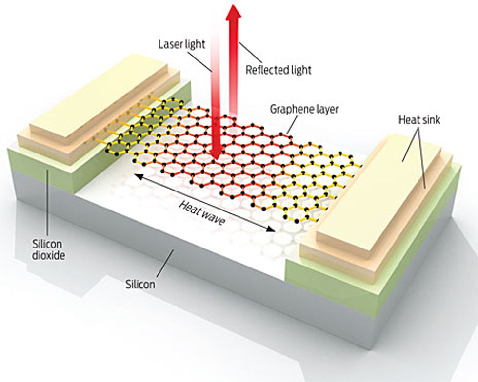
Illustration by Bryan Christie Design
Measuring the thermal conductivity of something with a thickness of just one atomic layer is tricky. At the University of California, Riverside, we approached the problem this way: First, we prepared samples to measure, each consisting of a long graphene flake suspended across a trench in a silicon wafer and attached to heat sinks. We then heated the graphene flake with a laser. The heat wave propagated from the middle of the graphene to the heat sinks.
To measure the temperature at the center of the hot spot, we came up with an unconventional use for a micro Raman spectrometer. Ordinarily, Raman spectroscopy is an optical technique used to identify materials. The Raman spectrum of graphene has a clear peak, referred to as a G peak; the spectral position of the peak depends on the temperature of the sample. So by measuring the exact position of the G peak, we were able to use our spectrometer as a thermometer.
Only a small portion of the laser light ended up dissipating in the graphene. Most of the light passed through it and was reflected back. We determined the fraction of the light dissipated in the sample by comparing the Raman intensity of the graphene with that of bulk graphite. Knowing the temperature rise, the dissipated light power, and the geometry of the graphene flake, we then determined the graphene’s thermal conductivity. The measured values exceeded 3000 watts per meter per kelvin near room temperature and depended on the size of the graphene flake. We learned later that our results agreed with physicist Paul G. Klemens’s predictions years earlier.
-Alexander A. Balandin