
Organic semiconductors have been intensely studied because they can be printed onto flexible plastic to produce large areas of cheap, durable circuits. But these circuits have been limited because charge moves through them at a snail's pace compared to the way it speeds through silicon.
The new technique, invented in the laboratory of Zhenan Bao at Stanford University, could lead to organic circuits that operate at frequencies up to four times as high as the best of today's organic devices. That's still barely one-hundredth the speed through crystalline silicon, but it would mean cheap printed organics could more easily substitute for amorphous silicon in displays and other gadgets.
Bao, an associate professor of chemical engineering, and her colleagues actually borrowed a trick called strain that is widely used in advanced silicon chips. Essentially, it involves stretching the semiconductor's crystal lattice in one direction and pinning it in place.
Bao's team worked with a widely researched organic semiconductor called TIPS-pentacene. You can think of it as a being shaped like a broad bar (the pentacene) with a ball on each side (the TIPS). Researchers like it because it can dissolve in solution, be printed like an ink, and then, when it dries, form crystals with relatively high charge-carrier mobility.
Pentacene is a p-type semiconductor, meaning that the charge is carried by holes, or electron vacancies. These holes hop from molecule to molecule when current is flowing, explains Bao. By putting the molecules under strain, Bao hoped to make them pack closer together and make it easier for the holes to hop. However, earlier attempts at adding strain could not get the molecules to hold their positions, because unlike silicon crystals, pentacene crystals are held together only by relatively weak forces.
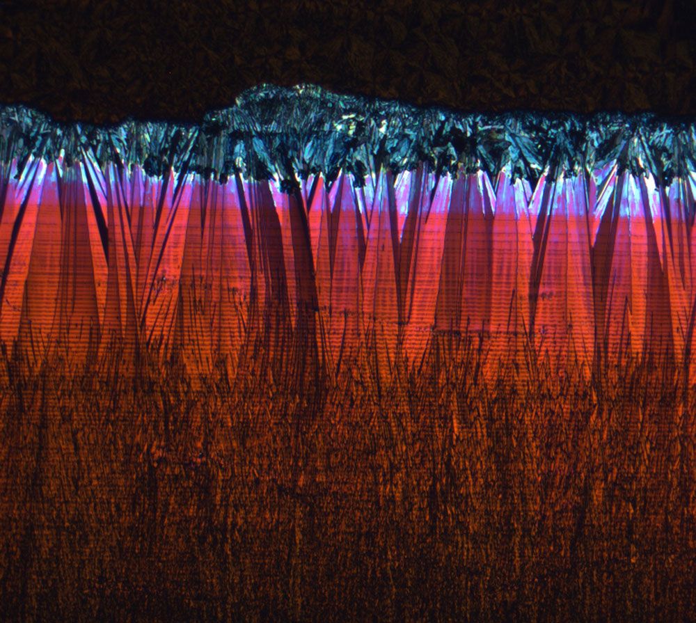
Bao's team induced strain in the material using a setup they'd developed years earlier. First they spread the semiconductor, dissolved in a solvent, over a temperature-controlled substrate. Then they used an angled plate, held at a fixed distance from the substrate, to smear the solution at a precise pace. As the knifelike shear plate moved along the surface, it pulled the molecules and induced the solvent to evaporate. The result was pentacene crystals strained in the direction of the moving plate.
"We hypothesized that shearing the solution would change the molecular packing," says Bao. "But we didn't know which way it would change." X-ray analysis of the material by Stefan Mannsfeld, a staff scientist at the Stanford Synchrotron Radiation Lightsource, showed that the TIPS-pentacene molecules were a little bit elongated and packed much more tightly in a crucial way.
"The molecules become closer in one direction," says Bao, "and slightly slide by each other in another direction." The parts of the pentacene through which charge moves were now 0.25 angstroms closer together, the team will report in tomorrow's issue of the journal Nature.
That might not seem like much, but it had a big difference on charge-carrier mobility. Under the best parameters, when the shear plate moved at 2.8 millimeters per second, the resulting semiconductors had an average mobility of 2.1 square centimeters per volt second, more than double what you get without strain. And the highest mobility they observed reached 4.6 cm2/Vs. (Increasing the speed of the shear plate further disrupted the crystal growth and led to declining mobility.)
"With further refinement we think we can get to the higher value" consistently, says Bao. That will involve achieving better control of how the TIPS-pentacene crystals nucleate and in which direction they grow.
Whether or not manufacturers will be able to make use of strain in their organic circuits is an open question. Researchers and companies have explored several printing methods including inkjet printing, but the kind of strain Bao's group developed probably won't be obtained with inkjet printing, says Yongtaek Hong, a professor of electrical engineering and computer science at Seoul National University, in South Korea. "The fundamental physics behind the research is really important," but "it would be difficult to apply to inkjet printing," he says. Among the problems are controlling the viscosity and evaporation rate of the jetted material to the degree they were controlled in Bao's experiments.
Last year Hong's research group reported that it had constructed an all-inkjet printed organic inverter circuit. However, Hong says the future of mass-manufacturing organic electronics is more likely to involve a roll-to-roll printing technique, in which materials are continuously coated or printed onto a roll of plastic as it is unwound and then wound up again.
Bao says her technique is probably compatible with that method. However, other researchers aren't so sure. Associate professor Annalisa Bonfiglio and postdoctoral researcher Piero Cosseddu, both in the electrical engineering department at the University of Cagliari, in Italy, say that reproducing the strain effect on reams of plastic won't be easy.
Bao's strained semiconductors were made on a rigid piece of silicon, so "the strain is entirely absorbed on the [organic] semiconductor surface," notes Bonfiglio, who has developed an organic-transistor-based strain sensor with Cosseddu and others, though that device works on a different principle than Bao's. But a flexible plastic substrate might absorb some of the strain and prevent the organic film from crystallizing correctly, she says.
The prospect of much faster organic transistors is so tantalizing that Hong thinks many groups will pursue ways to achieve the same strain result, even if they don't use Bao's technique. "If the organic thin-film transistor could get stable performance at 3 to 5 [cm2/Vs] mobility, it could get into high-performance displays" or complicated digital circuits, he says. Such displays, including 3-D TVs, have a refresh rate that is beyond the capabilities of today's organic transistors.
But with a little strain, maybe plastic 3-D TVs will be in our future.