
The silicon semiconductor industry has chugged along for more than 50 years. Like a steamroller, it has trundled over bumps and holes, while defying repeated warnings that it was running out of fuel or was about to be overtaken by flashier competitors.
So we technologists are understandably reluctant to speculate about the end of silicon. And yet, speculate we must. After decades of steady improvements to the efficiency and speed of our computer chips, brought about by physically shrinking the dimensions of silicon transistors, we’ve reached a point where the massive effort to miniaturize those switches ekes out only very modest gains in performance. The steamroller still rolls, but it’s slowing down, and the maintenance and upkeep on it are fast becoming unsustainable.
Researchers are pursuing many options to keep integrated electronics on its exponential arc. One possible approach is to simply give up on improving the silicon transistors themselves, and instead focus on changes to the architecture or design of computers. This strategy has had some success in the past, when, for example, we moved from single cores to multicore processors, or began incorporating specialized accelerators into systems. Yet there are only a limited number of design tricks that can be played, and we have used many of them already.
So future progress must still involve improving the underlying switches. Modifying materials and device geometries can create transistors with better electronic properties than silicon transistors have today. But such evolutionary approaches will yield only small benefits. To get bigger gains, we’re left with one option: use novel nanotechnologies to supplant silicon altogether.
There are many candidates for this role. But the most exciting and mature contender by far is the single-walled carbon nanotube, a rolled-up sheet of linked carbon atoms. If you’re experiencing some déjà vu now, it’s no wonder. There was great enthusiasm for carbon nanotubes in the 1990s, and a number of big-name semiconductor companies began investigating them. But the carbon nanotube fell out of fashion when researchers ran into obstacles in circuit fabrication that seemed too hard to overcome. When the first measurements of the electronic properties of graphene—flat lattices of carbon atoms—were reported in 2004, many were all too eager to abandon carbon nanotubes and take up that shiny new technology.
Now the carbon nanotube is back and better than ever. Unlike its much-hyped two-dimensional cousin, the carbon nanotube comes in a natural semiconducting form, which means it can be turned on and off to make a binary switch. And recent research into the material has moved well beyond the demonstration of simple logic gates. In 2013, for example, our group at Stanford University built the first complete digital system—a basic computer—entirely out of carbon-nanotube circuits. What’s exciting is that the fabrication and design techniques we employed to build that computer can be seamlessly integrated into a semiconductor fabrication facility today and used to manufacture chips with the billions of transistors needed to compete with state-of-the-art silicon.
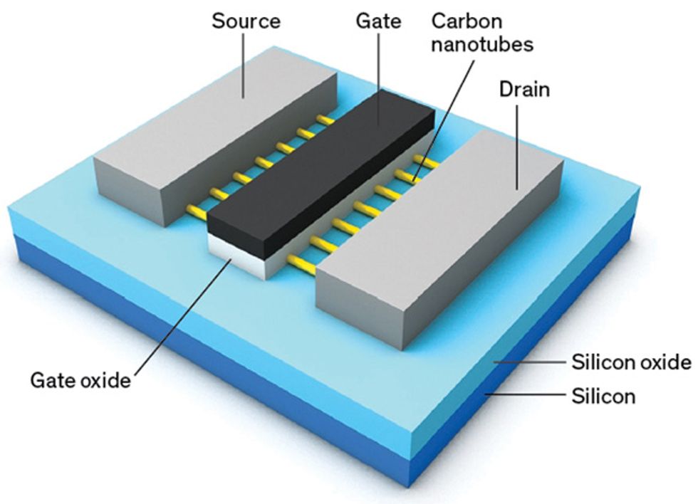 Switching with Carbon: A carbon-nanotube field-effect transistor (FET) resembles a conventional silicon FET. The main difference is the current-carrying channel, which is made from carbon nanotubes (yellow) instead of silicon.Illustration: Jean-Luc Fortier
Not only can carbon nanotubes make traditional chips more powerful, they can also be used to create entirely new computing systems—ultrafast and efficient three-dimensional chips that can be employed in data centers as well as the wide world of mobile computers used in cars, smartphones, and the sensor-filled Internet of Things. Such 3D systems could mix carbon nanotubes and emerging memory technologies, and they could also be built directly on top of conventional silicon circuitry. So while carbon nanotubes may eventually leap ahead of silicon, they could also share the road with it. In both cases, the resulting massive advances in computational capability would affect our lives profoundly.
The initial discovery of carbon nanotubes is hard to pinpoint in time. But many cite a landmark 1991 paper by physicist Sumio Iijima, who grew “graphitic carbon needles” on an electrode in a gas-filled vessel. Iijima’s work inspired a flurry of interest, and soon electrical engineers began suspecting that carbon nanotubes might be an ideal transistor technology.
To build a transistor, you need several things: a source and drain—the origin point and destination for current; a channel between the two where the current can flow; and a gate near the channel to control that flow. Semiconductor-device physics is complex, particularly when it comes to today’s nanoscale switches, but as a general rule of thumb, there are two basic properties that determine a transistor’s performance. First, the more current that flows through the channel, the faster a circuit can be. That’s because greater current allows the gate of the next device in the circuit to be charged faster. Second, the thinner the channel, the more energy efficient the device will be, because it will be easier for the gate to exert the control needed to turn the transistor on and off. Think of the channel as a water hose and the gate as your foot. The thinner the hose, the less effort you’ll need to make in order to stem the flow of water.
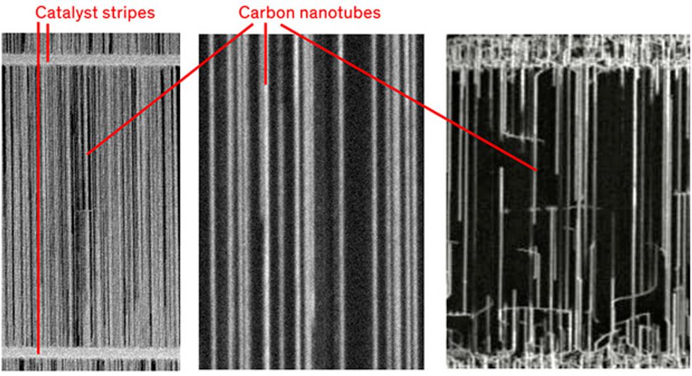 Straight and Narrow: Carbon nanotubes can be grown in parallel lines, but imperfections do occur.Photo: Max Shulaker
Unfortunately, in today’s ultrasmall silicon devices, these two factors—the thinness of the channel and the speed at which charge can flow through it—are at odds with each other. Like other three-dimensional bulk materials, as silicon gets thinner, the sides and edges of the crystal have a stronger and stronger effect on its electrical properties. These so-called surface effects impede the movement of charge through the material.
But the carbon nanotube naturally and simultaneously fulfills both of those transistor channel requirements. The nanotube’s smooth-walled structure is naturally devoid of dangling bonds, permitting charges to flow through it quite rapidly, many times faster than in silicon. And because carbon nanotubes are also very small—in the realm of about a nanometer in diameter—a gate can easily control the flow of current along its length.
A carbon-nanotube transistor looks much the same as a silicon transistor. The main difference is that the channel is made of carbon nanotubes instead of silicon. Just as in a silicon transistor, the electric field created by a gate controls the flow of current. And just as with silicon chips, circuits can be formed by connecting the carbon-nanotube transistors to one another with tiny metal wires built into additional layers of the chip.
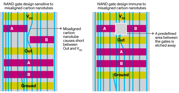 Tackling Imperfections: Carbon nanotubes don’t always grow in perfectly parallel lines. Some circuit designs are more sensitive to such imperfections than others. In the NAND gate design at left, for example, a wayward carbon nanotube can weave between gates, creating a short. Other designs, such as the one for the NAND gate at right, will function properly regardless of imperfections in the arrangement of the underlying carbon nanotubes.
Two independent teams, based at the Delft University of Technology, in the Netherlands, and at IBM, reported the first carbon-nanotube field-effect transistors (CNFETs) in 1998. And in the years after, researchers devised a number of experiments to probe the fundamental physical properties of these devices. They also began building basic circuits; a notable advance came in 2006, when an IBM group built a ring oscillator—a key logic demonstration circuit—by constructing 12 CNFETs from a single 18-micrometer-long carbon nanotube.
Impressive though those achievements were, there was a big gap between a small test circuit built from a single carbon nanotube and a chip that could compete with state-of-the-art silicon. To make a chip, researchers would have to find a way to construct billions of transistors from a sea of carbon nanotubes. A few requirements for high-performance circuits emerged early on. Each transistor channel would need to contain multiple, densely packed carbon nanotubes in order to drive enough charge to compete with the speed of silicon circuitry. What’s more, these dense carbon nanotubes should be spaced uniformly, minimizing electrical variation between transistors.
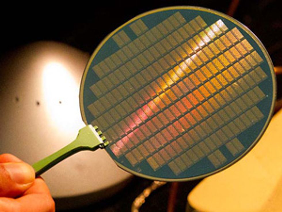 Wafer-thin: This wafer contains carbon nanotube circuitry. The fabrication techniques used to make those circuits could pave the way for more energy-efficient processors.Photo: Norbert von der Groeben
The natural way to reach this level of density and consistency is to build the sources, drains, and gates of the transistors on top of uniform arrays of closely spaced carbon nanotubes. But, as you might imagine, the process of creating a neat arrangement of billions of identical curled-up carbon sheets, distributed evenly on a silicon substrate, isn’t easy.
The problem begins with carbon-nanotube synthesis. Any process that is used to grow carbon nanotubes almost inevitably results in an assortment of tubes with different diameters and atomic arrangements. Variations in the underlying atomic structure yield carbon nanotubes with a mix of electrical properties. Some are semiconducting, while others are metallic. The semiconducting carbon nanotubes are exactly what you want for digital logic, while the metallic ones basically act as wires because they can’t be turned off by the gate. As a result, they always conduct current, even when the transistor should be turned off, which wastes power and can cause errors in logic operations.
To make matters worse, it’s hard to grow carbon nanotubes in nice parallel arrays on a surface. If some of them wind up in divergent orientations, they can extend beyond the confines of their own transistor channel and create random circuit connections. The density of nanotubes can also vary from spot to spot, which will result in transistors with a wide variety of current-carrying capacities. In fact, some could easily have no carbon nanotubes in their channel at all, resulting in device failure.
In 2004, our diverse group of students and postdocs at Stanford University, led by professors Subhasish Mitra and H.-S. Philip Wong, set out to tackle these problems. (One of us, Max Shulaker, began with the group in 2009 as an undergraduate and will soon join the faculty at MIT.) The field of carbon-nanotube research had shrunk significantly by the time we began our work. But the hope was that we, along with others in that small but innovative community, could finally figure out a way to transform the nanomaterial from a laboratory curiosity into the stuff of tomorrow’s chips.
Moving an Array
Transferring carbon nanotubes from quartz to silicon
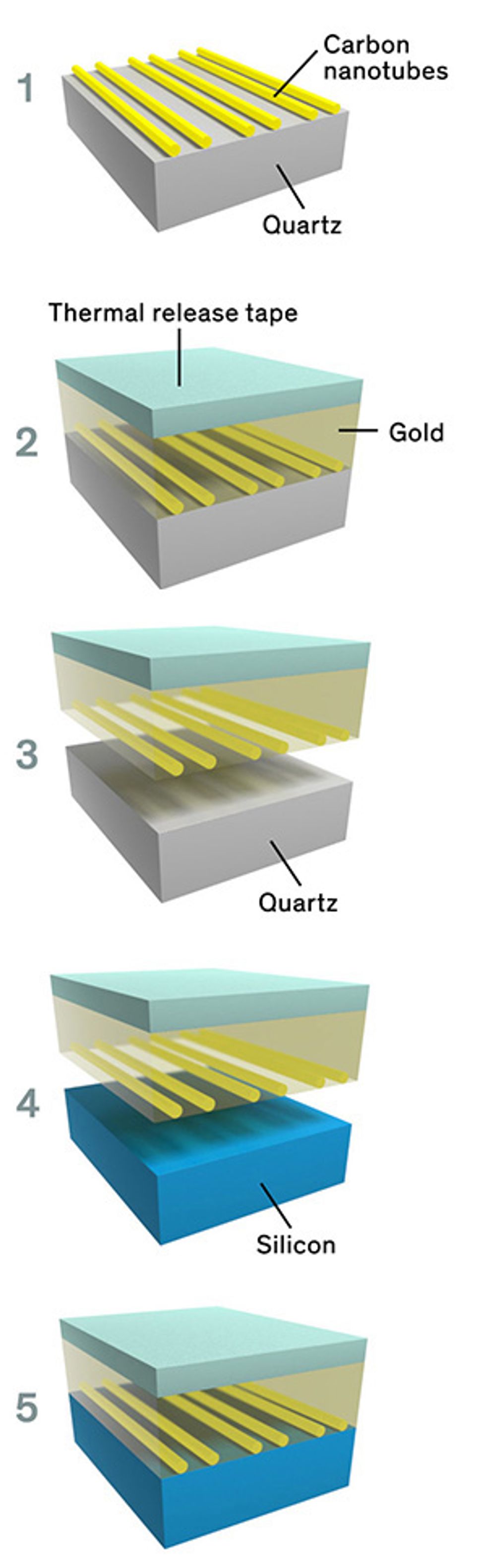 An array of carbon nanotubes can be grown at relatively low temperature on quartz (1). The array can then be transferred to a more traditional silicon wafer by using a metal layer deposited on top of the carbon nanotubes to pick them up (2-4). The metal is then chemically etched away, leaving the array behind on the silicon substrate.Illustration: Jean-Luc Fortier
To start, we focused on tackling two key obstacles to high-performance circuits mentioned earlier: the presence of misaligned carbon nanotubes and also of metallic ones. Our first step was to find a way to grow carbon nanotubes that were as aligned as possible. The approach we settled on, inspired by work done at the University of Illinois at Urbana-Champaign and the University of Southern California, was to grow them on a crystalline quartz substrate.
When surrounded by a carbon-rich gas, carbon nanotubes will grow out from metal nanoparticles stuck to the surface of a quartz wafer in nice, orderly parallel lines. We can then transfer the carbon nanotubes onto a more traditional chip substrate—an insulating layer of silicon dioxide on top of silicon—by coating the carbon nanotubes with a thin layer of metal. The metal acts as an adhesive, which we can then physically peel off the quartz and transfer to the silicon. This metal is then chemically etched away, leaving the array of highly aligned carbon nanotubes behind. (A similar transfer process is already used in commercial facilities to make silicon-on-insulator wafers for traditional chips.)
But even with quartz as a guide, we found that a small fraction—about 0.5 percent—of carbon nanotubes still do not grow properly. They might begin growing straight only to develop a kink and end up on a diagonal. To deal with these misaligned nanotubes, we devised a way to effectively design circuits around them. An automated design algorithm, based on graph theory, decides which areas of a circuit should be etched away so that it’s mathematically impossible for a stray nanotube to connect two electrodes that it isn’t supposed to. This scrubbing ensures that no misaligned carbon nanotube can cause a short circuit that interferes with the logic. Importantly, this process requires no knowledge of the exact positions of the aberrant carbon nanotubes—the same design works for any starting configuration. Without this strategy, we’d need to inspect every wafer and every carbon nanotube in order to find the misaligned ones, an impractical and costly process.
We found that we could tackle the metallic nanotubes with a similar mix of processing and design. In 2001, an IBM team showed that, with sufficient voltage, it’s possible to destroy metallic carbon nanotubes by burning them away. We adapted this technique to operate across an entire integrated circuit at once, by building temporary wiring that effectively turns a whole chip into one giant transistor. After the circuits are made, we apply a voltage to the gates of the transistors to turn off all the semiconducting carbon nanotubes. Then we apply a voltage across each source and drain region. Because the semiconducting carbon nanotubes have already been turned off, only the metallic nanotubes in the channels will conduct electricity. With a sufficiently strong voltage pulse, even the relatively low resistance of these bad nanotubes will create a brief heat spike that fries the nanotubes, turning them into minuscule puffs of C02. Today, we use a variation on this approach that can remove the entire length of a metallic carbon nanotube and eliminate more than 99.99 percent of them (a small and manageable fraction—now less than 1 percent—of the good, semiconducting carbon nanotubes are sacrificed in the process as well).
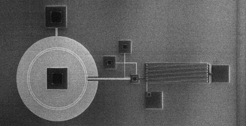
 Carbon Logic: A scanning-electron-microscope image shows a portion of the circuitry in the first carbon-nanotube computer, which the authors reported in 2013. The 1-kilohertz processor was primitive by modern standards, but it demonstrated that any digital system could be made using the devices.Illustration: Max Shulaker/Nature
Combining metallic-nanotube removal with our strategy for addressing misaligned nanotubes allowed us to build the first digital systems out of carbon nanotubes using only practical, large-scale manufacturing approaches (we refer to this combination of processing and design as the “imperfection-immune paradigm”). Our first proof of principle was Sacha, a handshaking robot that we demonstrated live at the 2013 IEEE International Solid-State Circuits Conference, in San Francisco. When a conference attendee grabbed the hand of the robot, a carbon-nanotube-based subsystem would sense the change in the value of an embedded capacitive sensor and trigger the robot to shake hands. While this was admittedly a simple show-and-tell demonstration, Sacha did make a very important point: CNFETs had reached a level of maturity where a live, system-level demonstration could be made.
To drive the viability of carbon-nanotube circuitry home, we also created a complete digital system: the first computer processor built entirely from CNFETs. The processor—which was built from only 178 CNFETs containing more than 30,000 carbon nanotubes—was certainly modest by modern standards. It used a 1-bit architecture and had a clock rate of 1 kilohertz, less than a millionth the clock rate of today’s CPUs. But we weren’t optimizing for speed; the chip was slow in part because we put probes at each node to monitor every possible transition inside the computer. Still, the processor was a complete computer; it could perform multitasking and emulate instructions from the commercial MIPS instruction set. More important, it showed that CNFETs could be used to build any kind of digital system, a first for any of today’s emerging nanotechnologies.
Of course, integration alone doesn’t make a technology. The performance of CNFET circuits was still far behind silicon. A core challenge here was carbon-nanotube density. At the time we reported our carbon-nanotube computer in 2013, we were able to grow arrays of carbon nanotubes with a linear density of 1 to 10 carbon nanotubes per micrometer, along the line perpendicular to the transistor channel. To create enough current-carrying capacity for a high-performance CNFET, we’d need 10 to 100 times that value. We’d also need to make sure that density would be uniform from spot to spot to keep transistor variations to a minimum.
 Circuits from Suspensions: Carbon nanotubes can also be processed in solution.Photo: IBM
In 2014, we reported a new technique that could simultaneously address those challenges. The approach builds on the strategy we used to move carbon nanotubes from the quartz substrate they’re grown on to the substrate that will be used to build a chip. We showed that this method could be used multiple times to layer one array of carbon nanotubes on top of another. Because it’s generally easier to make uniform arrays that are fairly sparse, this multiple-transfer approach also lets us decouple the density problem from the uniformity one. In other words, we can grow multiple sparse arrays and then layer them, one on top of the other, to achieve high density.
Unlike other potential nanoelectronic devices, the CNFETs we’ve made with this approach can deliver currents that are more or less on par with a silicon transistor of the same size. This was unprecedented performance for a carbon-based nanotechnology, and CNFETs are expected to get better still.
Ours isn’t the only approach to making carbon-nanotube circuitry. For example, IBM and several other research groups have done work with semiconducting and metallic nanotubes suspended in solution. The metallic nanotubes are separated and removed. Then the remaining nanotubes are dried on a substrate that has been patterned so that they land, as designed, in particular locations and orientations. Researchers are still working to drive down the fraction of metallic nanotubes that remain and boost the density of the semiconducting ones, but this method shows significant promise.
Despite advances like these, we still encounter skepticism when we talk about carbon-nanotube computing. One question that often arises is whether it’s possible to build complementary logic. Today’s processors use a semiconductor technology called CMOS, which stands for complementary metal-oxide semiconductor. The “complementary” refers to the fact that it employs two different kinds of transistors: n-type transistors, which carry electrons across the channel, and p-type ones, which use holes—positive charges that are actually an absence of electrons. There are many advantages to having both types of devices, but for years researchers primarily made only p-type carbon-nanotube transistors. That was because the first CNFETs were p-type and the materials used to make them are somewhat easier to work with. Indeed, our carbon-nanotube computer was made entirely from p-type CNFETs.
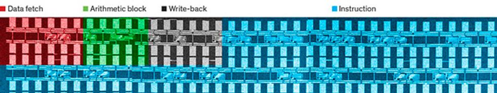 Metal and Carbon: A view of the 2013 carbon-nanotube computer’s circuitry shows various functional areas. More than 30,000 carbon nanotubes were used to create the computer’s 178 transistors.Image: Max Shulaker
But carbon nanotubes don’t intrinsically have a type, and it’s fairly easy to dope them to carry either charge carrier. Instead of inserting other types of atoms into the material, as is done in silicon, this doping can be done through the choice of materials used to make the insulating layer between the gate and the channel or the metal source and drain regions of the transistor. In the case of the source and drain, those materials essentially act as filters, permitting either electrons or holes into the carbon-nanotube channel. Many research groups, including our own, have used these approaches to create both n-type and p-type CNFETs. Moreover, we have demonstrated that these two devices can perform at comparable levels, an important consideration when designing circuits.
Another source of concern has been the electrical connections between carbon nanotubes and the metal source and drain contacts. When these connections aren’t perfect, they can have high electrical resistance, which consumes a lot of energy and slows computation. But this problem plagues any transistor as its dimensions get smaller and smaller. Pairing materials at the atomic scale is difficult and unforgiving. Fortunately for carbon-nanotube transistors, models suggest that we don’t need to have ideal contacts in order to make high-performance CNFET circuits. What’s more, recent work at IBM shows that big improvements can be made to the connection between carbon nanotubes and their metal contacts by essentially fusing the two materials, creating a near-seamless transition from carbon to metal.
We’ll have to bring together all these pieces of carbon-nanotube device fabrication, including doping and contact construction, if we hope to make these chips competitive with silicon. Further progress in decreasing variability will also be a priority, since a chip’s performance isn’t limited by its best transistors but by the worst ones. These are big challenges, but there will be a considerable reward for overcoming them. Models calibrated to experimental data suggest that, even with variations and other imperfections, microprocessors made from carbon nanotubes could outperform future silicon circuitry by a factor of 10 when it comes to the energy-delay product, or EDP, a metric of circuit speed and energy efficiency. The benefits will be even greater as transistors continue to shrink, because silicon devices will reach their size limit well before carbon-nanotube devices do.
Carbon nanotubes have other advantages, too. An emerging area of chip design is 3D monolithic integration, which creates a high-rise of circuits built directly on top of one another, connected by a dense forest of ultrafine vertical wires.
 Building Up: Circuits built one on top of another, connected by dense wiring, could dramatically improve speed and energy efficiency. This FPGA switching element (left) contains a carbon-nanotube transistor, a silicon transistor, and two resistive RAM memory cells. Each element sits on its own layer.Image: Max Shulaker
There is a strong motivation for this sort of structure. Today’s computers spend a very large amount of energy and time shuttling data inside a processor and between the processor and off-chip memory, across millimeters or centimeters of space. Today we can create 3D chips that mix logic and memory by making individual 2D silicon chips and then stacking and bonding them together. The layers are connected through extremely large and sparse vertical wires. Creating 3D structures with far denser connections would open up bottlenecks that exist today between logic and memory, which would greatly benefit applications that depend on processing vast amounts of data.
Such monolithic 3D integration is very difficult in silicon; the high temperatures commonly used to manufacture the transistors can melt metal wiring and damage the transistors beneath it. But the carbon-nanotube transfer technique we described earlier allows us to build circuits at temperatures that won’t damage underlying circuits. That’s because the approach essentially separates the high-temperature growth phase of the material—which happens at around 900 °C—from the rest of the circuit fabrication process. This isn’t speculation; we have already demonstrated several working CNFET-based monolithic 3D integrated circuits. The process is compatible with silicon and can even be used to add carbon-nanotube-device layers on top of a base of silicon transistors.
Projections suggest that combining carbon-nanotube transistors and emerging memory devices in a 3D system could yield a 100- to 1,000-fold benefit in energy efficiency over a traditional silicon chip with off-chip memory (this estimate assumes that both chips are manufactured with similar feature sizes).
Of course, as carbon-nanotube research continues, so do other efforts to make better transistors. A relatively new approach, the negative capacitance FET, uses material between the gate and the channel to boost the effect of the gate voltage, reducing the energy needed to switch. This design is compatible with carbon nanotubes and could be used to provide even greater benefits. Other alternative technologies, such as transistors that exploit electron tunneling and logic based on manipulating the spins of electrons, are also being pursued. But CNFETs remain the only emerging nanotechnology that has achieved such a high level of performance, complexity of system demonstration, and manufacturing maturity.
So when will we see this carbon-nanotube circuitry in our smartphones and data centers? Like any new technology, the carbon nanotube will merge onto the computing technology highway only if chipmakers decide to take it up in earnest. Thanks to these recent improvements in carbon-nanotube fabrication and design—and the fact that the material can actually complement silicon—that goal is becoming more and more realistic. This is one upstart that could overtake the silicon steamroller, if we’d only give it some gas.
This article appears in the July 2016 print issue as “Computing With Carbon Nanotubes.”
The authors would like to acknowledge the support of STARnet SONIC, DARPA, the National Science Foundation (NSF), and the Stanford SystemX Alliance.