
The integrated circuit could use a lift. Almost 50 years after Gordon Moore forecast the path toward faster, cheaper chips, we’ve miniaturized electronic components so much that we’re increasingly colliding with fundamental physical limitations. The days of simple transistor scaling are long behind us—the latest, greatest chips are a hodgepodge of materials and design tweaks. These chips also leak a lot of power, and they contain transistors that are so variable in quality they’re difficult to run as intended.
Fortunately, chipmakers are pursuing a pair of innovations that will give dramatic boosts in the two categories that really count: performance and power consumption. In both cases, the trick will be to build up and into the third dimension. And manufacturers will do it at the level of both the individual transistor and the full microchip. In 2012, the chip will start to become the cube.
Until recently, microprocessor transistors have been flat, built into the plane of the silicon. Each field-effect transistor on a chip contains four parts: a source, a drain, a channel that connects them, and a gate on top that controls the current flow through the channel. Only the gate and a thin layer of insulator beneath it sit above the silicon.

But this past May, Intel unveiled its plans for the first big move away from the planar transistor. After months of gearing up production, the new transistors, which are built into a processor code-named Ivy Bridge, will make their way onto the market during the first half of 2012.
The switch to these pop-up transistors—often called FinFETs—helps tamp down one of the key problems that have emerged as engineers have shrunk transistor dimensions: leakage current. The smaller a transistor, the weaker the gate’s control and the easier it is for current to sneak across the channel when the transistor is supposed to be off. Intel decided to go with a design that turns the transistor channel on its side, creating a protruding fin between the source and drain that can be controlled by a gate on three sides instead of one.
Expanding into the third dimension will let chipmakers continue shrinking transistors to boost speed, without leaking power. Indeed, Intel estimates the 22-nanometer Ivy Bridge chips will be 37 percent faster at low voltage and draw less than half the power of the company’s 32-nm chips.
Intel’s 3-D leap was anticipated, but its timing still came as a surprise. “Moving the technology from the lab to the fab is a big deal,” says Tom Halfhill, a senior analyst at the Linley Group, in Mountain View, Calif. Based on available road maps, Halfhill says, other chipmakers working on FinFETs are a good four to five years behind Intel. “As far as we know, nobody else is close to volume production,” he says.
Intel’s FinFET isn’t the only foray out of Flatland. In 2012 there will be solid progress on an even more promising trick: stacking chips and wiring them together with interconnects that run straight down the stack, like elevator shafts in a skyscraper. If all goes well, this reworked interconnect technology could yield vastly faster and more efficient devices, no matter how chunky their transistors might be.
In some ways, 3-D is nothing new to chipmakers. Flash memory, for example, is stacked to cut down on volume and boost speed. But chip stacking has been limited by wiring problems. Today’s interconnects don’t run through the silicon itself but instead go millimeters around it, impeding speedy signaling and sapping power along the way. Horizontal real estate is also precious. The thinnest interconnects are still 25 micrometers wide, and they must be packed along the edges of a chip, putting strict limits on how many input/output connections any one chip can handle.
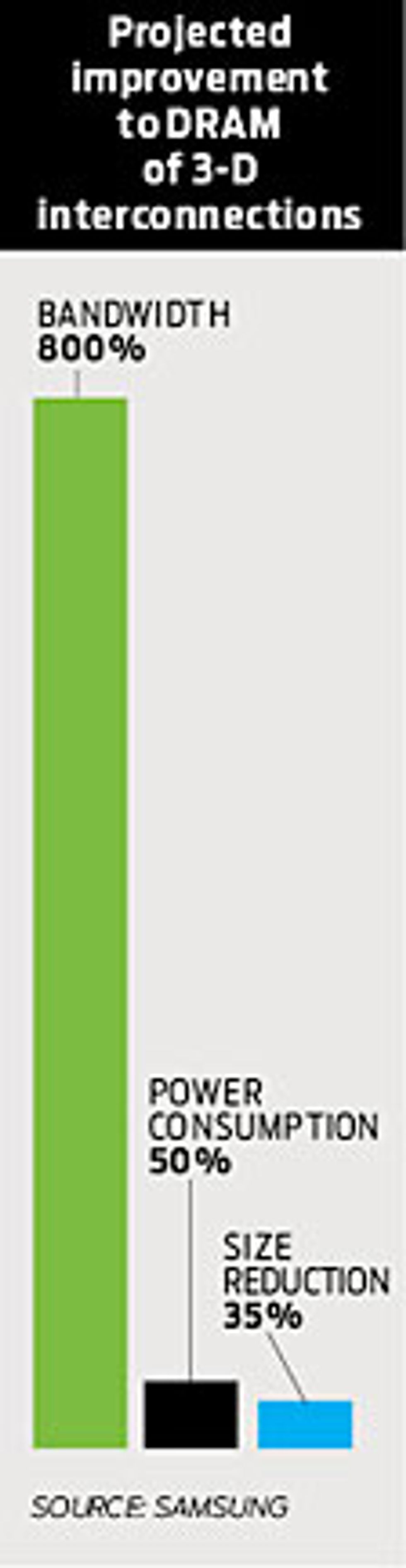
Thus the attractiveness of going vertical, connecting one chip to another with copper lines that go straight through the silicon. If chipmakers can cheaply manufacture these through-silicon vias (TSVs), they can pack many more connections side by side using much slimmer wires. Going through chips instead of around the side will also reduce the length of interconnects from millimeters to 50 μm or even less—as thin as individual wafers can be made. The potential advantages are huge. Samsung, one of several companies working on making dynamic RAM memory stacks connected by TSVs, has estimated that the switch to vertical interconnects will cut power consumption in half, increase bandwidth by a factor of eight, and shrink memory stacks by some 35 percent.
“It’s really phenomenal that you can do something like that,” says Sitaram Arkalgud, who directs the 3-D interconnect program at Sematech, a semiconductor industry consortium. “It’s not often that you see this kind of a revolution come along.”
To build TSVs, a wafer maker has to etch deep, narrow holes into a silicon wafer and then fill them with a nearly flawless layer of insulating material and then copper. But as a wafer heats up, copper expands at more than five times the rate that silicon does, exerting stress that can crack the wafer and render it useless.
Shepherding these wafers through the chip manufacturing process is also a challenge. Each wafer must be thinned to roughly 50 μm, less than the thickness of a human hair. Wafers that thin can curl up like pencil shavings. To work with them, chipmakers have to temporarily attach them to plates that can stabilize them during processing.
But industry watchers say that most of the main technical hurdles have now been overcome. This year, companies will be working out ways to introduce TSVs without adding significantly to the cost of making a chip. This is “the year we figure out how to make them manufacturable. It’s the year of process development and yield improvement,” says industry consultant E. Jan Vardaman, president of TechSearch International, in Austin, Texas.
In fact, the most dramatic achievement in the coming year might be a simple stacking configuration that’s often called 2.5D. This approach takes advantage of TSVs by running them through an intermediate layer of silicon called an interposer, which sits between an IC and a PC board. By one measure, the technology is more or less two-dimensional. All the packages you choose to put in a device—RF receivers, graphics units, memory, logic—still sit on the plane of the motherboard. But instead of copper traces running across the motherboard from package to package, in this configuration copper connections run through TSVs and past the interposer layer, where the vertical wiring is connected in a series of horizontal patterned layers. By moving all the connections outside the plane, device makers can place chips right next to one another, saving space and power.
One of the pioneers of interposer technology is Xilinx, in San Jose, Calif., which has used TSVs to wire together four field-programmable gate arrays to form the world’s largest FPGA. This programmable pachyderm contains nearly 7 billion transistors, easily 50 percent more than the biggest single FPGA, Xilinx says. The firm estimates that the device consumes less than a fifth of the power that would be needed to operate a comparable set of individually packaged FPGAs strung together with traditional copper interconnects.
Vertical stacks of TSV-enabled chips are not far behind 2.5D technology. Elpida, Micron, Samsung, and Toshiba are all in various stages of creating memory stacks built with TSVs. Some of these companies have already shipped prototype chips to customers, and industry watchers expect TSV-based high-end memory—the sort that would be useful for servers and high-performance computers—to emerge in 2012.
“We’ll see [TSVs] start to come out in applications where cost is not the main concern but performance is,” says Jim Walker, a vice president of research at Gartner who follows packaging developments.
Memory chips are a natural entry point for new 3-D technology because they are more tolerant of thermal stress, Walker says. Chipmakers, he says, still haven’t found a good way to carry heat out of the middle of a stack. The problem is particularly thorny when the stacks contain different chips. “The graphics chip is like an oven,” Walker says. “If you’re putting memory or RF die on top of it, you’ll have different heat generators with different thermal expansion rates.” The result is degraded chips that don’t run as well or as long as they should.
There are other big questions that will need to be addressed as manufacturers contemplate making more complicated chip stacks. How do you make sure that two chips made by different companies can be connected? Is there an inexpensive way to verify that each layer in a package works? And if the finished IC doesn’t work, how do you determine who is responsible for the failure?
Foundry giant Taiwan Semiconductor Manufacturing Co. (TSMC) has been struggling with this last question as the company tries to ramp up interposer production by its target date in the second half of 2012. “When we started TSV development, we did it the conventional way,” says Doug Chen-Hua Yu, who heads up interconnect and packaging R&D at the company.
Yu says TSMC typically sends completed wafers to be packaged by assembly companies known as OSATs (outsourced subassembly and test providers). But the thinned wafers are too easily damaged. When that happens, “it’s very hard to go back and decide who did what wrong,” Yu says. “It [could be] the wafer fab or the OSAT or FedEx. We don’t know.”
Even if wafers are inspected carefully before and after shipping, there could be latent damage that emerges only after processing. As a result, Yu says, TSMC is now hoping to do most of its TSV wafer manufacturing and packaging in-house.
Liability issues, industry standards, and a host of other manufacturing matters still need to be sorted out. But no one seems to foresee any insurmountable hurdles to 3-D TSV technology. “It’s changing how we do the whole supply chain. That’s why it’s taking such a long time to get this on the ground and running,” says Sematech’s Arkalgud. “But once it happens, it will be going for quite some time.”
This article originally appeared in print as “ICs Grow Up.”