A team of researchers based in Switzerland is on the way to laying bare much of the secret technology inside commercial processors. They pointed a beam of X-rays at a piece of an Intel processor and were able to reconstruct the chip’s warren of transistors and wiring in three dimensions. In the future, the team says, this imaging technique could be extended to create high-resolution, large-scale images of the interiors of chips.
The technique is a significant departure from the way the chip industry currently looks inside finished chips, in order to reverse engineer them or check that their own intellectual property hasn’t been misused. Today, reverse engineering outfits progressively remove layers of a processor and take electron microscope images of one small patch of the chip at a time.
But “all it takes is a few more years of this kind of work, and you'll pop in your chip and out comes the schematic,” says Anthony Levi of the University of Southern California. “Total transparency in chip manufacturing is on the horizon. This is going to force a rethink of what computing is”, he says, and what it means for a company to add value in the computing industry.
Even if this approach isn’t widely adopted to tear down competitors’ chips, it could find a use in other applications. One of those is verifying that a chip only has the features it is intended to have, and that a “hardware Trojan”—added circuitry that could be used for malicious purposes—hasn’t been introduced.
The work, which was published this week in the journal Nature, was conducted at the Paul Scherrer Institute’s Swiss Light Source. The facility is a synchrotron; it accelerates electrons that are moving close to the speed of light in order to generate beams of X-rays.
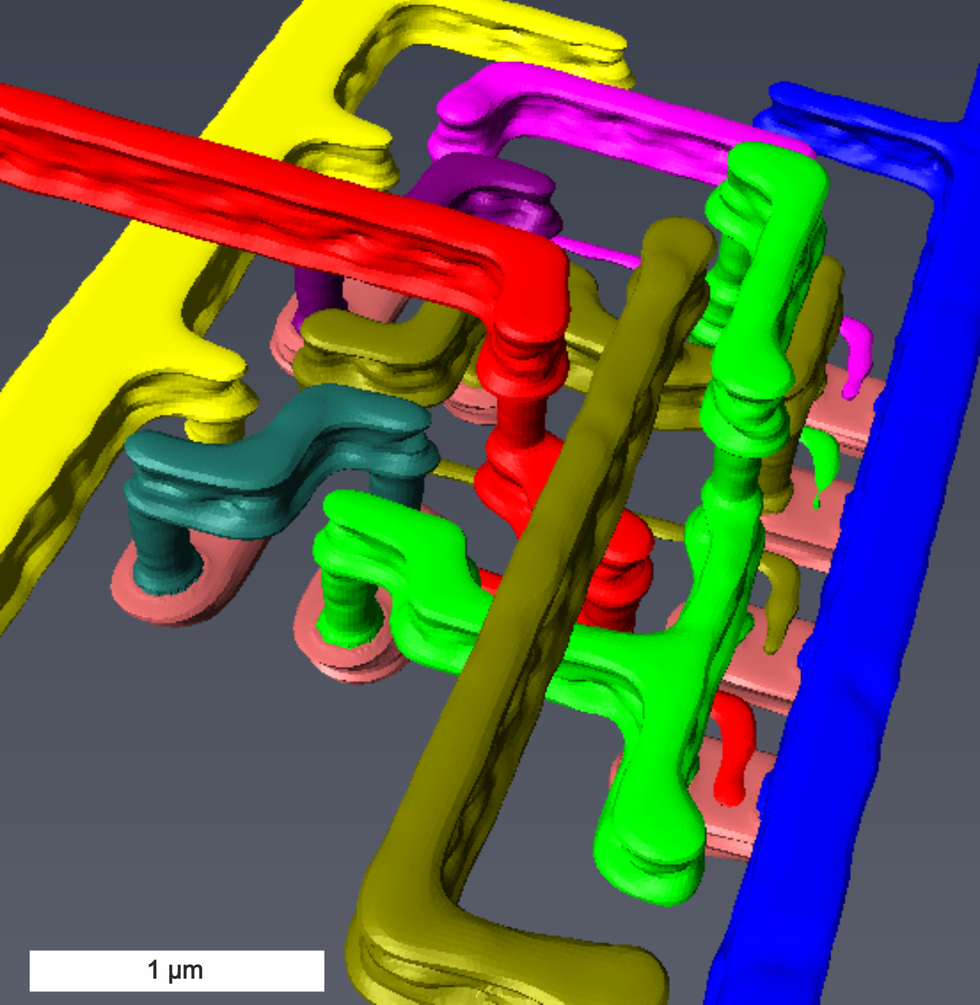
To produce a 3D rendering of the Intel chip—an Intel G3260 processor—the team shined an X-ray beam through a portion of the chip. The various circuit components—its copper wires and silicon transistors, for example—scatter the light in different ways and cause constructive and destructive interference. Through a technique called X-ray ptychography, the researchers could point the beam at their sample from a number of different angles and use the resulting diffraction patterns to reconstruct chip’s internal structure.
They began their experiments with a chip they knew the structure of—an ASIC developed at the institute to read out data from a light detector. The team found an excellent match between the chip design and their measurements, and they were able to identify and study the features of a particular circuit inside the chip in fine detail.
 A reconstruction of a set-reset latch in the ASIC chip that the team imagedImage: Mirko Holler
Then they moved on to image circuitry inside the Intel processor, about which they had limited information. The ASIC was produced using 110-nanometer chip manufacturing technology, more than a decade from being cutting edge. But the Intel chip was just a couple of generations behind the state of the art: It was produced using the company’s 22-nm process. (Intel then jumped to 14nm and 10nm is now in the works.)
The resolution for this technique in any one direction is 14.6 nm, which rended individual transistor components fairly blurry. The resolution can be improved, but it may be a race to stay close to the smallest features in the chip industry: per Moore’s Law, chip dimensions have gotten smaller since 22nm and continue to do so.
This is not the first time that researchers have attempted to use X-rays to image the interior of integrated circuits, says team member Gabriel Aeppli. But “the resolution is better than it’s been in the past. The scale is also larger,” he says. “It’s a huge chunk of the chip compared to what you could do with any other technique.”
In this proof-of-concept, the team was using an experimental set-up that was optimized for cylindrical samples, and they had to carve a 10-micrometer-wide pillar out of the chip in order for the imaging process to work. But in the future, the group aims to move toward a different geometry that will allow them to image circuitry without having to damage the chip.
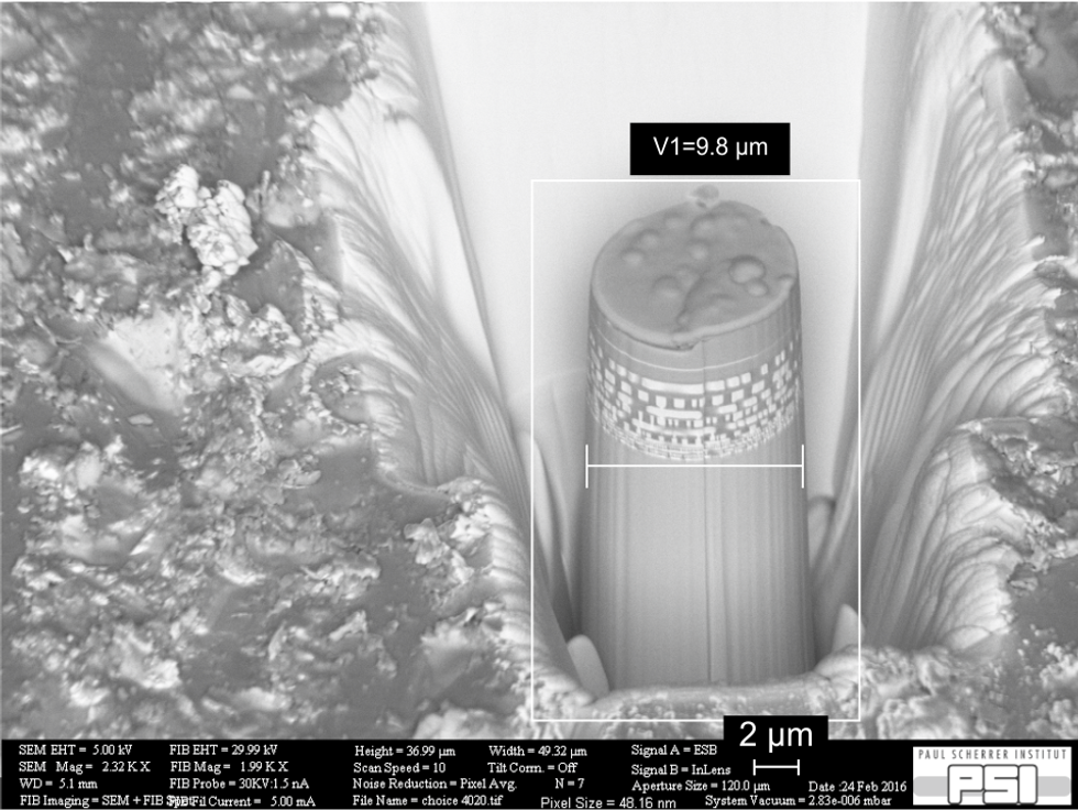 A view of a 10-micrometer-wide pillar carved from the Intel G3260 processor, prior to its extraction. The team expects that changes to the experimental geometry will allow them to image circuitry without cutting into chips.Image: Mirko Holler
The imaging itself was no small feat. The sample has to remain stable, and interferometers must be used to continuously measure its position. It took about 24 hours to perform the X-ray measurements and the data processing took about as long, says team leader Mirko Holler. But additional computers should easily speed the processing, he says. And improvements to X-ray sources as well as other parts of the experimental apparatus could improve the imaging speed by a factor of 1000.
“I don’t see any other probe that could image a full processor without slicing it up,” says Jerry Hastings, a professor at the SLAC National Accelerator Laboratory in Menlo Park, Calif. “You need something that simultaneously gives you the resolution and the penetrating power. And that’s where X-rays are unique.”
“What they’ve done is a proof of concept and it’s quite impressive at that level”, says Dick James, an emeritus fellow at TechInsights, which strips chips down to the transistor level to examine how the devices are built and wired together.
James says there are practical limitations to the amount of circuitry that can be analyzed using those traditional tear-down techniques, which, depending on the packaging, can start with a bath in boiling sulphuric acid. But he notes a lot can be gleaned by piecing together small electron microscope pictures of the chip: “You can get most of the cell library by looking at smaller areas.”
And even with a perfect image of an entire chip, there will be some things you can’t know about how the chip was made. “So many steps are sacrificial,” James says. “Unless there’s some sort of residue or fingerprint left by a process, you can’t actually see what’s been done. You just have to infer it from the structures that are left behind.”
Although X-ray ptychography does promise bigger, high-resolution views, it faces several obstacles, James says. For one, chip feature sizes at the cutting edge could prove a challenge for its resolution. “The industry is getting ahead of this technique already,” he says. Another impediment is the need for a synchrotron source. These aren’t likely to find their way into chipmaking fabs, although there are a number of such facilities around the world and it is possible to rent time on them.
Because of these limitations, James says, the best application for this imaging technique could be on chips that are made with older manufacturing processes, and thus have larger features. This is the case for a number of chips used in military and space applications. “If you can look at the whole chip, then you can compare the chip with the original design,” James says, and “do a direct comparison [to] see if there are any obvious faults or any extra circuitry that’s been put in.”
A version of this post appeared in the May 2017 print magazine as “3D X-ray Tech for Easy Reverse Engineering of ICs.”