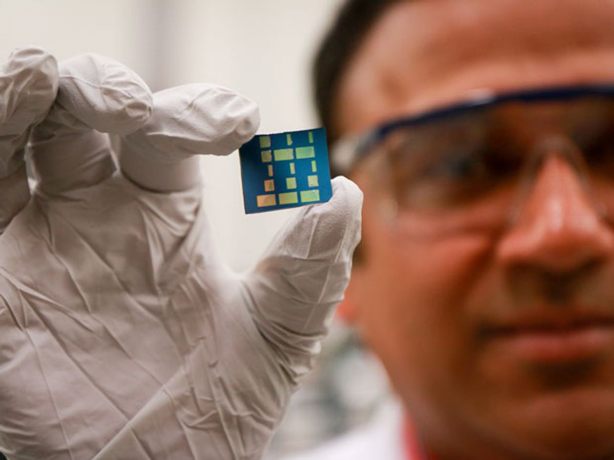
Researchers at the University of Utah have developed the first stable intrinsic p-type (carrying positive charges) 2-D semiconductor material, tin oxide. If this semiconductor is mated with a n-type (carrying electrons) 2-D semiconductor in a transistor, it opens up the possibility of building power-saving two-dimensional complementary logic circuits like the ones in microprocessors today.
"Now we have everything—we have p-type 2-D semiconductors and n-type 2-D semiconductors," said Ashutosh Tiwari, an associate professor at the University of Utah and the leader of the research, in a press release. "Now things will move forward much more quickly."
The potential for 2-D materials—such as graphene and molybdenum disulfide—as an alternative to the three-dimensional silicon, raises hopes for smaller, faster, lower-power transistors.
However, the path to success for these 2-D materials in transistors has not always been clear, whether it be issues such as graphene not being a natural semiconductor or the charge carrier traps that compromise molybdenum disulfide. But possibly the biggest issue has been that all previous 2-D materials have only been stable n-type semiconductors. It has been possible to dope other 2-D materials, such as molybdenum disulfide and tungsten diselenide, to behave as p-type. However, this new tin oxide represents the first intrinsic p-type semiconductor in a 2D material.
In research described in the journal Advanced Electronic Materials, the Utah University researchers overcame this limitation by layering 2-D tin oxide (SnO) onto a sapphire-and-silicon-dioxide (SiO2) substrate. The researchers were then able to fabricate a few field-effect transistors (FETs) from it.
With this development, the attractive properties of 2-D materials in transistors are more fully exploitable. For instance, in 2-D materials charge transport is basically confined to a single plane, meaning electrical and thermal transport properties that can be much better than those of bulk silicon. That could mean chips that consume less power and throw-off less heat.
In an e-mail interview, Tiwari said that the next step in their research will be to build a CMOS (complementary metal oxide semiconductor) using their new p-type 2-D semiconductor.
This post was corrected on 18 February to indicate that some 2-D materials could act as p-type semiconductors when doped.
Dexter Johnson is a contributing editor at IEEE Spectrum, with a focus on nanotechnology.


