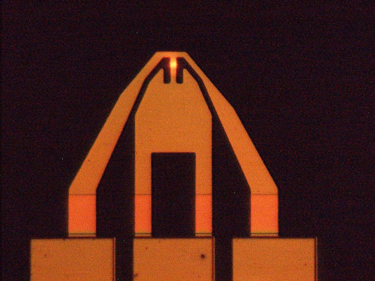
In their manufacturing of the tip, the researchers took as their inspiration the way in which steel is strengthened through tempering. They exposed the silicon tips typically used in these devices to carbon ions and then annealed them so that a silicon carbide layer was formed while still maintaining the sharpness of the original silicon tip.
This is not the first time this team has pushed the capabilities of AFM tips. Last year the researchers developed silicon oxide-doped diamond-like carbon tips.
At the time, those tips represented the state-of-the-art, with their wear-resistance at the nanoscale being measured as 3000 times greater than silicon. The latest design is 10 000 times more wear resistant at the nanoscale.
IBM's press release quotes University of Pennsylvania professor Robert W. Carpick as saying that "compared to our previous work in silicon, the new carbide tip can slide on a silicon dioxide surface about 10 000 times farther before the same wear volume is reached and 300 times farther than our previous diamond-like carbon tip.This is a significant achievement that will make nanomanufacturing both practical and affordable."
The researchers believe that this new super-hard tip will open up new application areas for probe-based technologies like biosensors for measuring glucose levels. This is due to its ability to resist wear when being slid across the surface of silicon dioxide.
Mark Lantz, manager in storage research at IBM Research-Zurich predicted that the technology will be used in microscopic sensors that monitor "everything from water pollution to patient care."
While biosensors may be the longer range goal of the research, which was published online on 8 February in the journal Advanced Functional Materials, the researchers will initially look to put the tip to work in nanomanufacturing and nanolithography applications.
Dexter Johnson is a contributing editor at IEEE Spectrum, with a focus on nanotechnology.


