Since 2008, James Tours’ research group at Rice University has been championing its discovery that silicon oxide can form the basis of resistive memory. In the past four years, there have been a fair number of doubters who just couldn’t believe that silicon oxide could switch its resistance, but there has also been a growing body of research from other labs that corroborates that four-year old work.

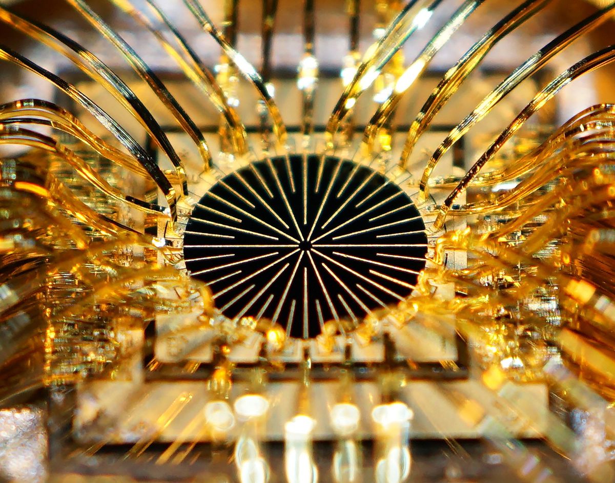
The core of the new memory chip is the use of silicon oxide that has been sandwiched between layers of graphene and placed on flexible plastic sheets. While the Rice researchers have been looking at the use of graphene in flexible displays of late, in that work nanowires were sandwiched between the layers of graphene. In this latest research, silicon oxide is sandwiched between the graphene layers.
In fact, it has been the Rice team’s nanowire-and-graphene research—and its dogged belief in silicon oxide’s ability to switch its resistance and serve as a resistive memory—that has made this latest development possible. In the 2010 paper that followed their 2008 discovery of silicon oxide’s capabilities, Yao observed that running a voltage through silicon oxide removed oxygen atoms from the material creating a 5-nanometer-wide channel, and turned it into pure silicon filaments.
When Yao reversed the voltage, he discovered that the silicon filaments could be broken and reformed, creating a “0” for a broken circuit and a “1” for the healed circuit—the basis of computer memory. Since then Yao has been attempting to build up evidence that the switching effect he witnessed was not a result of the breaking graphite but because of the underlying crystalline silicon.
“Jun was the first to recognize what he was seeing. Nobody believed him,” says Tour in the press release. “Jun quietly continued his work and stacked up evidence, eventually building a working device with no graphite.”
To quiet the doubters, who believed that the switching had to be due to some carbon in the system, Yao created a device that had no exposure to the carbon at all. The devices that the Rice team is producing now contain no metals except for the leads attached to the graphene electrodes.
Tour further notes: “Now we’re making these memories with about an 80 percent yield of working devices, which is pretty good for a non-industrial lab When you get these ideas into industries’ hands, they really sharpen it up.”
The history of nano-enabled, non-volatile memory's challenges to flash memory have proven to be less than successful in the past, but this could be an architecture that changes that trend.