Ever since the 1980s, when Gerd Binnig of IBM first heard that “beautiful noise” made by the tip of the first scanning tunneling microscope (STM) dragging across the surface of an atom and later developed the atomic force microscope (AFM), these microscopy tools have been the bedrock of nanotechnology research and development.
AFMs have continued to evolve over the years, and at one time, IBM even looked into using them as the basis of a memory technology in the company’s Millipede project. Despite all this development, AFMs have remained bulky and expensive devices, costing as much as US $50,000.
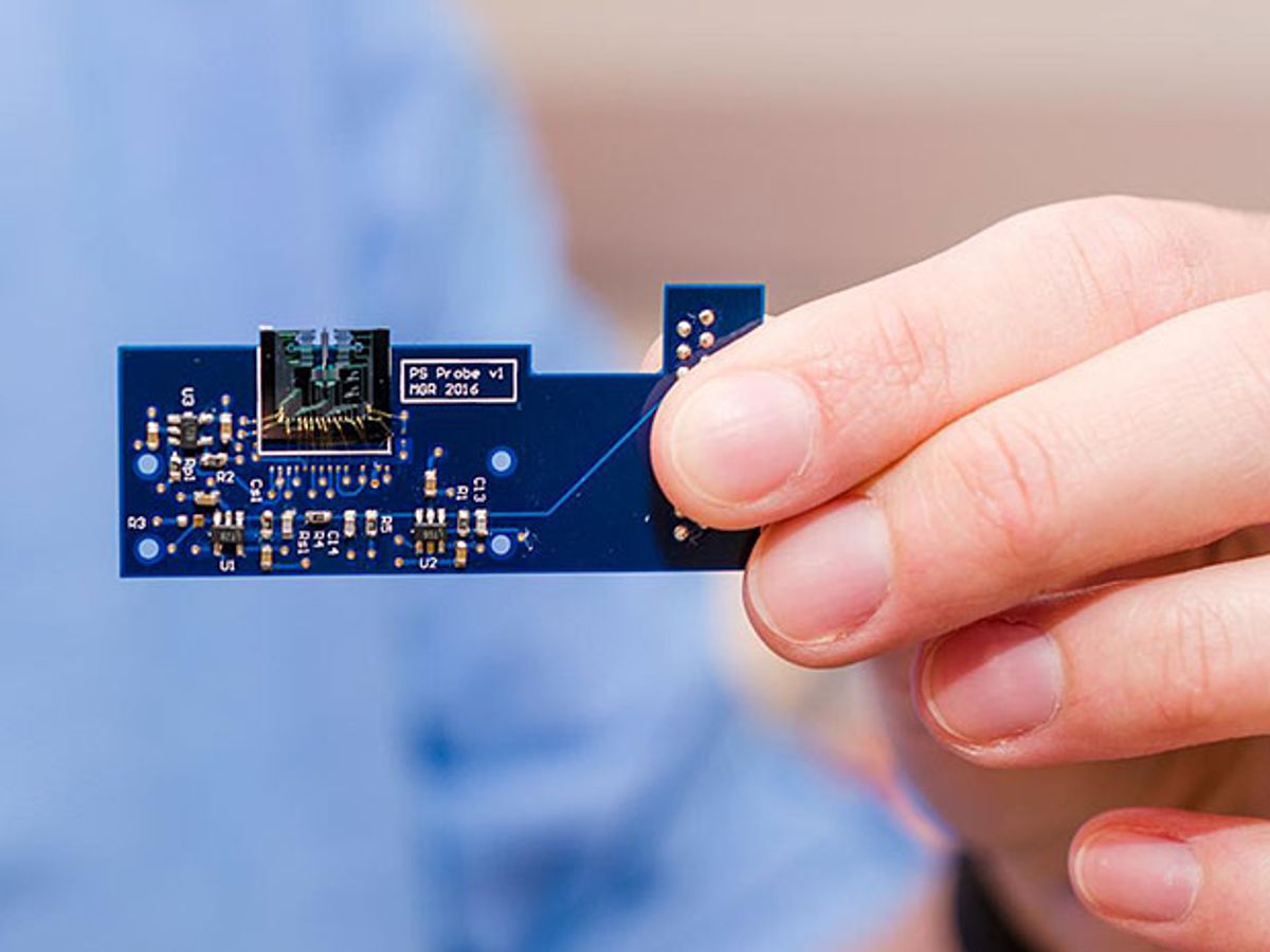
Now, researchers at the University of Texas (UT) Dallas have turned this paradigm on its ear by developing an AFM that uses microelectromechanical (MEMS) technology. The upshot: The entire AFM fits onto a computer chip about one square centimeter in size.
In research described in the journal IEEE Journal of Microelectromechanical Systems, the scientists connected the MEMS-based AFM to a small printed circuit board containing all the circuitry, sensors, and other miniaturized components that control the device’s movements.
While the reduced size, and the likely lower cost associated with the economies of scale for MEMS devices look to be the clearest benefits, it is in how these AFMs take their measurements that truly sets them apart from previous AFM technology. AFMs have always mapped the surface of a material by recording the vertical displacement necessary to maintain a constant force on the cantilevered probe tip as it scans a sample's surface.
Instead of depending on a constant force or distance, the tip of the device developed by the UT scientists oscillates up and down perpendicular to the sample, touching and then lifting off of the surface—a mode known in AFM circles as the “tapping mode". This technique stands in stark contrast to the widely used contact-mode AFM. The UT researchers have developed a novel approach to implementing the tapping mode in an AFM by using a single piezoelectric transducer simultaneously for actuation and sensing, which removes the need for using an optical sensor.
Since the amplitude of the oscillation wants to change as it interacts with sample, this atomic force microscope creates an image by maintaining the amplitude of oscillation.
“Performing the measurement in tapping mode reduces the forces applied to the sample, which is important when scanning fragile samples such as biological specimens,” explained Reza Moheimani, professor of mechanical engineering at UT Dallas and coauthor of the research, in an email interview with IEEE Spectrum.
In tests of the prototype MEMS AFM, the UT Dallas researchers introduced samples into the AFM using the same approach mechanism of a commercial macroscale AFM. The printed circuit board containing the MEMS device was lowered onto the samples using a stepper motor.
“We imagine that a final version of the system would use a similar approach, with a compact motorized mechanism being used to bring the MEMS die in contact with the sample from above,” says Moheimani.
Because the sample would have to be prepared in a similar way as current AFM imaging, the setup would not need to be in a vacuum, Moheimani says. “At this stage, imaging within a liquid environment is not feasible with this device. However, future iterations of the MEMS AFM may be designed with this capability in mind,” Moheimani adds.
The prototype MEMS AFM was designed so that it could be fabricated using a straightforward MEMS process, with all mechanical scanning and sensing components contained in a single silicon-on-insulator MEMS die.
“There were significant challenges in designing the device to comply with the requirements of the fabrication process while obtaining the desired characteristics in terms of mechanical bandwidth, displacement range, and cross coupling,” says Moheimani.
The UT Dallas researchers had to employ an iterative design process in which the testing and characterization of an earlier fabricated version of the device allowed them to better exploit the capabilities of the fabrication process and significantly improve performance in areas such as cross-coupling reduction and reliability of signal routing.
Moheimani and his colleagues already have their sights set on the next engineering challenges for the MEMS AFM. For instance, the sharp probe at the end of the MEMS AFM’s cantilever is fabricated in a postprocessing step using electron beam deposition. The researchers are currently working to integrate the fabrication of the probe into the MEMS fabrication process. This will simplify the fabrication of the device and improve its durability.
Additionally, the researchers are looking to miniaturize the supporting electronics and control systems. They’re trying out prototype hardware in conjunction with an application-specific integrated circuit (ASIC) that interfaces with the MEMS die. This would make it possible to connect with the end user’s PC via a single USB connection.
Moheimani adds: “Our ultimate aim is to develop a system that can perform video-rate AFM imaging using a single MEMS chip. The current device successfully demonstrates many of the capabilities required, and future iterations of the device will be designed to further work towards this goal. Such a device would enable high-speed AFM imaging to be performed using a portable and cost-effective system.”
Dexter Johnson is a contributing editor at IEEE Spectrum, with a focus on nanotechnology.


