Research has been increasing over the last couple of years in using DNA nanostructures for combining top-down and bottom-up approaches to help the semiconductor industry keep feature sizes of chips on their ever-downward trek.
The first I reported on this trend was when IBM two years ago this month announced the use of DNA origami structures as a sort of scaffold for attracting carbon nanotubes to them and thereby creating miniature circuit boards.
Earlier this year, researchers Hongbin Yu and Hao Yan at Arizona State University got all the trade press covering their research, which developed a way to ensure that DNA origami was placed where you wanted it to be on the silicon by using “nano islands” made from gold. The latest technique using DNA origami uses the molecules for the masking and etching of silicon.
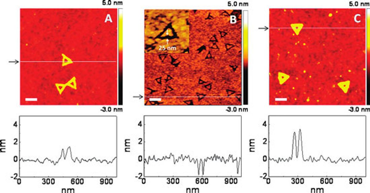
The research, which was originally published in the July 13, 2011 online issue of Journal of the American Chemical Society,exploits the ability of DNA to both promote and inhibit etching of SiO2 at the single-molecule level.
"Our approach to pattern transfer for bottom-up nanofabrication is based on the discovery that DNA promotes/inhibits the etching of SiO2 at the single-molecule level, resulting in negative/positive tone pattern transfers from DNA to the SiO2 substrate," Haitao Liu, an assistant professor in the Department of Chemistry at the University of Pittsburgh, explains in the Nanowerk article cited above.
"DNA nanostructures can be made with precise control over their sizes and shapes. Their use as lithography mask, however, has been limited due to their poor chemical stability. Our work provides a way to transfer the shape of the DNA nanostructure to silicon wafer, with sub-20 nm resolution."
In the research conducted thus far, the researchers were able to create 20-nm trenches, which could be used as nanofluidic channels, but the process is currently not optimized. However, the researchers believe that if a thinner layer of SiO2 film is used that a “patterned SiO2 layer could be used as a mask for etching of the underlying silicon substrate.”
"The formation of the trench indicates that the DNA origami locally increases the rate of oxide etching under these conditions" explains Liu in the Nanowerk Spotlight piece. "The full width at half-maximum of the trench (16.7 ± 2.8 nm) is comparable with the edge width of the DNA origami, indicating an overall faithful pattern transfer process. This result is consistent with our hypothesis that DNA can increase the etching rate of SiO2 by increasing the concentration of water. The small width of the trench shows that this effect is indeed spatially localized around the DNA."
While the researchers move on to sub-10nm structures, it would seem that perfecting this process is some ways off.As the Nanowerk story concludes, we get: “The major challenges in this undertaking are the issue of how to further increase the contrast of the transferred pattern and, crucially, to increase fidelity, consistency and accuracy of the process.”
One might term all these increases as developing “manufacturability.” It seems like it’s kind of a long way off. We may be pinning a lot of hope on a process like this if we’re looking for it to step up and take up the challenge of getting feature sizes below that of photolithography and e-beam lithography.Dexter Johnson is a contributing editor at IEEE Spectrum, with a focus on nanotechnology.


