One of the holy grails of graphene research has been a method for achieving wafer-scale growth of wrinkle-free single-crystal monolayer graphene on a silicon wafer.
Now researchers at the RIKEN research institute in Japan have discovered that the wrinkles in graphene may be their most attractive feature.
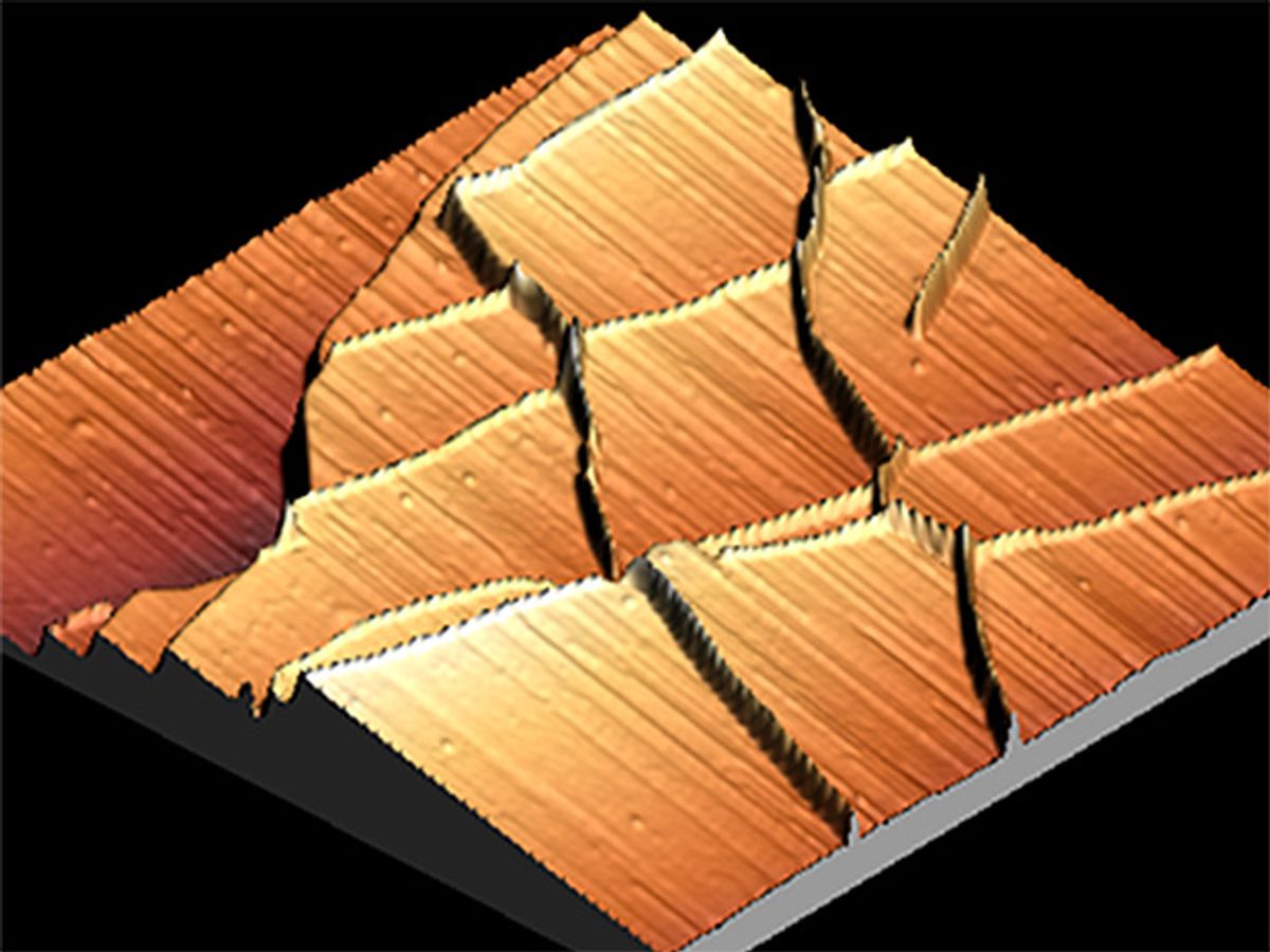
In research published in the journal Nature Communications, the RIKEN scientists discovered that the wrinkles found in graphene create unique electronic qualities, specifically a one-dimensional electron confinement. This restriction of electron movement results in a junction-like structure that changes from a zero-gap conductor to a semiconductor and back to zero-gap conductor.
The other revelation yielded by this research is that it’s possible to manipulate the wrinkles to change graphene’s band gap using mechanical methods rather than chemical techniques.
“Up until now, efforts to manipulate the electronic properties of graphene have principally been done through chemical means, but the downside of this is that it can lead to degraded electronic properties due to chemical defects,” said Yousoo Kim, who led the RIKEN team, in a press release. “Here we have shown that the electronic properties can be manipulated merely by changing the shape of the carbon structure. It will be exciting to see if this could lead to ways to find new uses for graphene.”
The discovery that it was possible to produce graphene semiconductors without the need to chemically dope the carbon sheets was the result of trying to produce graphene films using chemical vapor deposition (CVD). They were attempting to use CVD to grow graphene on a nickel substrate; they were examining how they could control the process with changes in temperature.
“We were attempting to grow graphene on a single crystalline nickel substrate, but in many cases we ended up creating a compound of nickel and carbon, Ni2C, rather than graphene,” explained Hyunseob Lim, the paper’s lead author, in a press release. “In order to resolve the problem, we tried quickly cooling the sample after the dosing with acetylene, and during that process we accidentally found small nanowrinkles, just five nanometers wide, in the sample.”
When examining the wrinkles with a scanning tunneling microscope, the researchers discovered that there were band gaps within them, which meant that they could act as semiconductors.
Dexter Johnson is a contributing editor at IEEE Spectrum, with a focus on nanotechnology.


