The team of researchers, including those at Georgia Institute of Technology along with others from Leibniz Universität Hannover in Germany, the Centre National de la Recherche Scientifique (CNRS) in France and Oak Ridge National Laboratory in the United States, has developed a process for producing graphene nanoribbons on a silicon wafer that results in such high electron mobility that the electrons behave more like photons do when in an optical fiber.
The lack of inherent band gap in graphene—its inability to effectively stop and start the flow of electrons—has remained a major stumbling block in developing it for use in electronics. Of course, there have been various approaches to engineering a band gap into graphene, such as applying a strong electrical field to bilayer graphene. However, Walt de Heer, a Regent's professor in the School of Physics at the Georgia Institute of Technology, believes that we should stop trying to get graphene to behave like silicon, and instead design a new type of electronics that exploits graphene’s unique properties. This is along the lines of what Samsung proposed 18 months ago by developing new switches to exploit graphene’s electron mobility.
As a first step in this quest, the researchers have developed a novel way to produce graphene nanoribbons, which previously have been investigated as a way to achieve a band gap in graphene. Prior to this most recent work, one of the ways you could produce a band gap in graphene was to reduce the dimensionality of graphene nanoribbons from two dimensions down to one dimension. In this way you would open a band gap through the 1-D confinement of electrons. However, to open a band gap large enough for electronic applications, the graphene nanoribbons would have to be reduced to widths of 2 nm. This was really not a practical way to produce a band gap in graphene.
However, in this latest work the researchers were not trying to achieve a band gap in graphene nanoribbons. They were just developing a method for getting graphene nanoribbons down on a silicon wafer. When they measured their results, they discovered that the graphene nanoribbons behaves more like an optical waveguide and allows electrons to flow smoothly along the edges of the material. The result is that in 40 nm-wide graphene nanoribbons ballistic transport exceeded the theoretical conductance levels of graphene by a factor of 10.
"This work shows that we can control graphene electrons in very different ways because the properties are really exceptional," said de Heer, in a press release. "This could result in a new class of coherent electronic devices based on room temperature ballistic transport in graphene. Such devices would be very different from what we make today in silicon."
The researchers, who published their findings in the journal Nature (“Exceptional ballistic transport in epitaxial graphene nanoribbons”), grew the graphene nanoribbons epitaxially—a process in which crystals are grown on a substrate, in this case, silicon carbon wafers. The silicon carbon wafers that served as the substrates had patterns already etched into them using standard microelectronic fabrication techniques. When the wafers are heated to 1000°C, the silicon is preferentially driven off along the edges, leaving behind graphene nanoribbons that have been given a structure determined by the pattern of the three-dimensional surface.
In this pattern, "[i]t seems that the current is primarily flowing on the edges," says de Heer. "There are other electrons in the bulk portion of the nanoribbons, but they do not interact with the electrons flowing at the edges."
The team discovered that it was possible to disrupt the flow of electrons in the graphene nanoribbons simply by attempting to measure the flow with an electrical probe. In fact, if you touched the nanoribbons with one probe, you would double the resistance; two probes would triple it.
"This should enable a new way of doing electronics," de Heer said in the release. "We are already able to steer these electrons and we can switch them using rudimentary means. We can put a roadblock, and then open it up again. New kinds of switches for this material are now on the horizon."
Of course, the researchers concede that even theoretical explanations of what the researchers have measured have not been completed, and a great deal of fundamental physics still needs to be done, but it does point to a new direction for applying graphene to electronics.
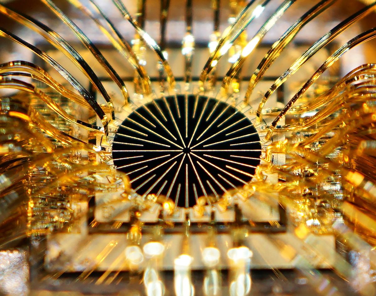
Illustration: John Hankinson