The end appears nigh for scaling down silicon-based complementary metal-oxide semiconductor (CMOS) transistors, with some experts seeing the cutoff date as early as 2020.
While carbon nanotubes (CNTs) have long been among the nanomaterials investigated to serve as replacement for silicon in CMOS field-effect transistors (FETs) in a postsilicon future, they have always been bogged down by some frustrating technical problems. But, with some of the main technical showstoppers having been largely addressed—like sorting between metallic and semiconducting carbon nanotubes—the stage has been set for CNTs to start making their presence felt a bit more urgently in the chip industry.
Peking University scientists in China have now developed carbon-nanotube field-effect transistors (CNT FETs) having a critical dimension—the gate length of just 5 nanometers—that would outperform silicon-based CMOS FETs at the same scale. The researchers claim in the journal Science that this marks the first time that carbon-nanotube CMOS FETs under 10 nanometers have been reported.
More important than just being the first, the Peking group showed that their CNT-based FETs can operate faster and at a lower supply voltage than their silicon-based counterparts.
At a 0.4-volt supply voltage, the current that flows through the CNT transistor is larger than what you’d get from the best silicon CMOS transistors at a 0.7-V supply voltage, according to Peking University’s Lian-Mao Peng in an email interview with IEEE Spectrum. (The “best” according to Peng is Intel’s 14-nm-node CMOS.) Because the gate’s capacitance is smaller for a carbon-nanotube transistor, even if the silicon devices were scaled down to the size of the CNT device, the latter would still switch faster, he says. The intrinsic delay caused by the gate capacitance for 10-nm CNT CMOS is about 70 femtoseconds, says Peng. That’s just one-third of the value (220 fs) of 14-nm silicon CMOS.
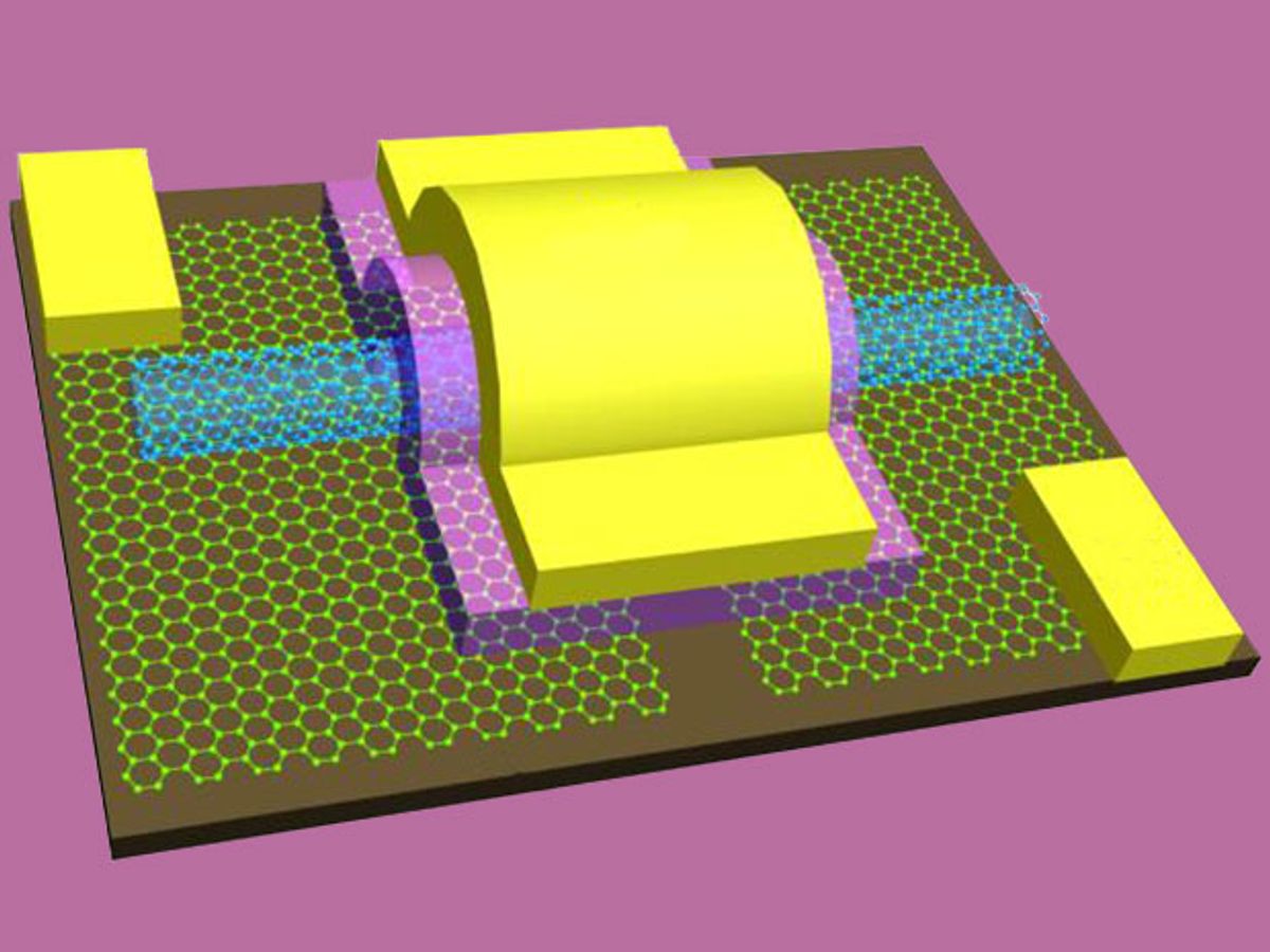
As with all the field-effect transistors, current flows through a channel between the source and drain under the control of voltage at the gate. In the Peking design, the channel through which the carriers move is made out of a single carbon nanotube and the source and drain are both graphene. This CNT channel is either p-type—conducting positive charge carriers, or holes—or n-type, which uses electrons. It is this combination of the p-type and n-type devices that constitutes the “complementary” of CMOS and keeps power consumption low when switching logic states.
Unlike most carbon-based and two-dimensional devices, the CNT FETs that the Chinese researchers have developed are not “back gated.” Back-gated devices—in which the gate electrode lies beneath a layer of insulation and the nanotube lies atop the insulation—are generally more difficult to integrate into complicated circuits.
Instead, the device Peng and colleagues constructed uses a gate that drapes over the top of the carbon-nanotube channel. “Top-gated FETs can provide higher gate efficiency than the back-gated devices since the CNT is almost surrounded by the top gate,” says Peng. “Also, top-gated FETs provide better stability than back-gated devices since the CNT channel is protected from influences of the outside world by the top gate.”
While the researchers concede that the use of individual single-walled carbon nanotubes to construct their devices is not suitable for producing large-scale integrated circuits, they are confident they can overcome this without changing much.
“Now that we have confirmed the potential of CNT CMOS transistors in the work, we can construct CMOS FETs with similar performance on aligned CNT arrays with high density and high semiconducting purity using the same fabrication process.”
With the ability to scale down silicon CMOS petering out in the coming years, there is some question as to whether there is enough time to replace silicon, or whether it is even worth the effort.
“We believe CNT electronics have a good chance to replace [silicon] CMOS technology at 5-nm nodes by 2022,” says Peng. As optimistic as Peng is, he remains cautious about the engineering challenges that they still face.
“While we can use the currently available CNTs…to fabricate large-scale CNT ICs, it still requires one to two years to get the ideal CNT form for ICs,” he says. Nonetheless, Peng believes that they will be able to make wafers full of ICs in the next few years using their process.
Dexter Johnson is a contributing editor at IEEE Spectrum, with a focus on nanotechnology.


