With each passing day, the limitations of silicon chips become increasingly pressing. The inexorable march of Moore’s Law to smaller and smaller dimensions in order to double the number of transistors on integrated circuits every two years is beginning to sound like the footsteps of an army of giants. Despite brilliant engineering twists and tweaks, eventually silicon is not going to be able to avoid getting crushed by this onslaught, at least not without some help from other materials.
The problems with silicon are not just limited to an inability to meet the demands put on it by the shrinking dimensions of chips. It’s also not particularly good at a number of things that would be nice capabilities. For instance, you can’t really get silicon to emit light for photonic applications, and silicon circuits can’t withstand temperatures beyond 250 degrees Celsius. This last limitation requires all sorts of complicated engineering of the circuits to account for its temperature sensitivity.
But now, researchers at the University of California Davis have found a way to combine silicon with nanowires to create circuits that not only will make possible smaller dimensions, but also emit light for optoelectronic applications and withstand high temperatures found in hostile environments such as inside a jet engine.
"Silicon can't do everything," said Saif Islam, professor of electrical and computer engineering at UC Davis, in a press release. "In the foreseeable future, society will be dependent on a variety of sensors and control systems that operate in extreme environments, such as motor vehicles, boats, airplanes, terrestrial oil and ore extraction, rockets, spacecraft, and bodily implants.”
While combining silicon with non-silicon materials has offered more robust performance, it has remained a challenge to grow non-silicon materials as layers over silicon because of incompatibilities in the crystal structures and differences in thermal properties.
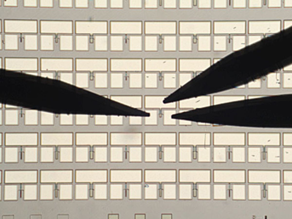
To overcome this limitation, Islam has grown nanopillars from gallium arsenide, gallium nitride, or indium phosphide on top of the silicon to serve as foundations on top of which nanowires are used to bridge the gap between the nanopillars.
"We can't grow films of these other materials on silicon, but we can grow them as nanowires," Islam explained in the release. In the video below, Islam explains how nanowires can be grown on silicon and can improve its capabilities.
In research, which was published in the journal Advanced Materials (“3D-Transistor Array Based on Horizontally Suspended Silicon Nano-bridges Grown via a Bottom-Up Technique”), Islam and his colleagues developed a bottom-up technique to create these nanowire bridges. They note that it does not require the tedious nanowire alignment and contact formation processes that are typically required to connect these nanowires.
This bottom-up approach led to the researchers being able to get the nanowires to operate like transistors and form the basis of more complex circuits. The material also proved to be responsive to light.
Perhaps most attractive to the semiconductor industry is that the technology does not require any significant changes to the manufacturing of silicon integrated circuits.
Dexter Johnson is a contributing editor at IEEE Spectrum, with a focus on nanotechnology.


